SCDA038 September 2021 TMUX7308F , TMUX7411F , TMUX7412F , TMUX7413F , TMUX7462F
2 How Does a Fault Protected Multiplexer Protect the System
In the first section of this report some common issues are discussed that plague designers when they are designing Analog Input Modules for PLC’s. This section will delve into a potential solution for the protection needs of the Analog Input Module – Fault Protected Switches/Multiplexers from TI. To understand the benefits of using a Fault Protected Switch/Multiplexer in a system’s Analog Input Module each of the aforementioned problems will be compared to TI’s Fault Protected Switch/Multiplexers features to see how these devices will be able to protect the system from possible fault conditions.
The Fault Protected Multiplexer or Switch is implemented into an Analog Input Module by placing the IC between the signal input, such as a sensor or external connector, and the signal conditioning/ signal processing blocks. The Switch/Mux IC can either connect one input to one signal conditioning block or connect multiple inputs into the same signal conditioning block. This is shown in Figure 2-1 where the blue diagram shows a multi-channel 1:1 switch and the red diagram shows a single channel 2:1 multiplexer as an example of how the signal chain + mux/switch look in general.
 Figure 2-1 Generalized Analog Input Module With Switch/Multiplexer
Using the basic architecture from Figure 2-1 the fault conditions can be analyzed. The first fault condition that will be examined is the case where there is a generalized voltage transient on the input of the analog input module. The transient is characterized by voltages that exceed the rated input range with either an undervoltage or overvoltage event. TI’s Fault Protected Switches and Multiplexers are built with voltage protection for both over and under voltage events. For example, the TMUX7308F, an 8:1 multiplexer, has the following specifications, with fault protection features bolded:
- +/-5 V to +/-22 V Dual Supplies
- 8 V to 44 V Single Supply
- Passes Rail to Rail Signals
- 8:1 Multiplexer
- Latch-Up Immune
- +/- 60 V Voltage Protection Under Powered Off Conditions
- +/- 60 V Voltage Protection w.r.t. Ground
- +/- 85 V Voltage Protection from Source to Supply
- +/- 85 V Voltage Protection from Source to Drain
- Non-Fault Channels Will Operate Normally
The five fault protection characteristics are shared by many faults protected multiplexers – although actual rating may change – so be sure to verify with the specific devices’ data sheet. Each of these specs are important in understanding max ratings for the device in a specific use case.
With respect to the fault condition of a generalized transient event – this fault specifically is dealing with overvoltage and undervoltage protection. For Fault Protected Switches and Multiplexers there are three ratings to pay attention to. The first is voltage rating with respect to ground and the second is voltage rating from source to supply/ source to drain. For the ratings there is a simple process that you can do to calculate the protection boundaries with these two specs.
Find Minimum Voltage with Equation 2.
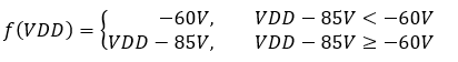
Then the maximum can be found in a similar way as shown in Equation 3.
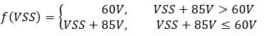
This will give a good idea of overall bounds of protection for the part – however, there is one more condition that needs to be understood which is the Source to Drain voltage measurement. A simplified example is shown in Figure 2-2.
") Figure 2-2 Multiplexer with Two Inputs (S1 Closed, S2 Opened)
Figure 2-2 Multiplexer with Two Inputs (S1 Closed, S2 Opened)For this 2:1 multiplexer there a few things to note – the source pins (S1, S2) are connected to VIn1 and VIn2 respectively. The supplies are VDD and VSS. The drain pin is D and is connected to S1 which means that the voltage at the drain and S1 are the same. This puts a limit on the voltage that can be on S2 as the +/-85V spec applies from source to drain as well. Using Equation 4, will determine whether or not there will be an issue:

As a quick recap of the information a couple quick examples can be shown to help build understanding.
Example 2.1 What are the protection bounds when VDD = 20V and VSS = -10V?
Using Equation 5

Using Equation 6

In example 2.1 the min and max bounds for the protection circuitry on the IC is -60V to 60V.
Example 2.2 What are the protection bounds when VDD = 30V and VSS = -5V?
Using Equation 7

Using Equation 8

In example 2.2 the min and max bounds for the protection circuitry on the IC is -55V to 60V.
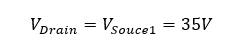
Example 2.3 Using Figure 2.2 as reference what are the bounds on VIn2 (V_Source2) when VDD = 40V, VSS = 0V and VIn1 (V_Source1) = 35V.
Using Equation 2

Using Equation 10

When in spec the following equation is valid because VSource1 is connected to the output.:
Using Equation 12 to solve for VSource2 yields the following two equations:
This gives a preliminary range of Vin2 to be from -50V to 120V. However, since the device has other limits on min and max inputs this range will be shrunk down to -45V to 60V to keep in line with the other device specifications.
These examples show that TI’s Fault Protected Switches and Multiplexers can handle a wide range of over/under voltages that can change based on a few designer choices. This is not the full story though. While it has been shown how to calculate protection boundaries, the next step to discuss is how and when these devices react. This comes down to three simple concepts: fault levels, fault thresholds, and output state during fault. Fault levels are set in two ways depending on device. If the device has a VFN and VFP pin, the fault levels can be set by placing supplies between these pins and ground such as with the TMUX7462F (4 channel, 1:1 channel protector which has its switches closed unless VDD = 0V or a fault condition is detected). If the device does not have VFN and VFP pins the fault levels are set to VDD and VSS voltages as is the case with devices like the TMUX7308F. These devices will not react until the input signal is either above or below a set fault level by a threshold voltage Vt (typically ~0.7V). When a fault level has been exceeded by the threshold voltage or more the device will react. How it reacts depends on device. Some devices such as the TMUX7308F will disconnect the fault channel and “open” the output and provide no overshoot on the output – a block diagram of this concept can be seen in Figure 2-3 and an oscilloscope capture of the output of the TMUX7308F is shown in Figure 2-4.
 Figure 2-3 TI Fault Protected Multiplexer, Open when Fault Occurs Shown
 Figure 2-4 No Overshoot on Output When Fault Detected
However, some devices such as the TMUX7462F provide a DR pin that allows a choice of output states during a fault condition. While also being able to open the channel with a fault the device can also be used to clamp the output to the supply. These two parts match the two patterns that emerge in TI’s Fault Protected Switches and Multiplexers which include the TMUX73XXF and TMUX74XXF families.
The next protection feature needed is that of protection against live signals into a system that is unpowered. This is simply a matter of getting a multiplexer/switch with powered off protection as a feature. This means the switch will be high-impedance until an active VDD is present – this will be rated within a range of voltages – for the TMUX7308F for example this is +/-60V which means that when VDD = 0V a signal of +/-60V on the input pin will not cause damage. However, there is still some leakage current that will conduct through the switch and these values can be found in the respective IC’s data sheet, however there will be no current that leaks through either VDD or VSS as there is no direct connection from inputs to VSS or VDD, so there shouldn’t be an issue of back-powering when using devices with powered-off protection.
Another need from a fault protected front end mux or switch is to be able to protect from overvoltage’s and undervotlage’s that can occur due to a shifting ground reference from excess ground current – this is also called ground shifting. An analog input system can have multiple IC’s connected to the same ground, commonly referred as the system ground. Ideally these ground connections all form one node that has 0V between any ground connection. This is not the case in reality – as there is a small impedance between ground connections. Under normal operating conditions it is generally safe to assume that these are all at the same potential – but in the case of a large ground current, these references can shift. However much in how TI’s Fault Protected Switches and Multiplexers protect against voltage transients it also protects against electrical overstress due to ground shifting. The best way to show this is with a quick example.
 Figure 2-5 TMUX7462F in Generalized Analog Input Module
Example 2.4: Find the States of S1, S2, S3, and S4 in Figure 2-5 with the following Parameters:
Using the TMUX7462F as the switch with the following parameters.
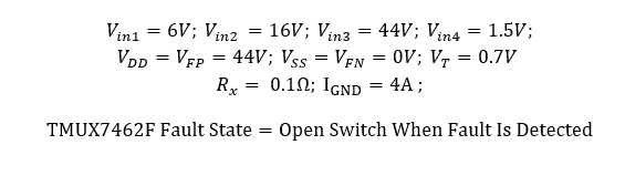
First, the TMUX7462F’s VSS/GND voltage w.r.t. system ground voltage needs to be found. This can be done by multiplying the current I_GND by the series resistance between VSS/GND and the system ground. For this example, Rx is 0.1Ω and I_GND is assumed to be 4A this leads to the equation 5*Rx*I_GND = 5*0.1Ω*4A = 2V. With this value the TMUX7462F’s VDD to VSS voltage can be calculated to be 42V w.r.t. to system ground and can accept values between 2V and 44V w.r.t. system ground.
Now that VDD-VSS has been found for the TMUX7462F the ground nodes for the input voltages need to be found. Using the same process as for VSS it can be seen that VINX_GND w.r.t. GND = X * Rx * 4. Which result in the following: Vin1_GND = 0.4V; Vin2_GND = 0.8V; Vin3_GND = 1.2V; and Vin4_GND = 1.6V. This now allows for the max and min Vin which has results in Table 2-1.
| Input | Max | Min |
|---|---|---|
| VIN1 | 6.4 V | 0.4 V |
| VIN2 | 16.8 V | 0.8 V |
| VIN3 | 45.2 V | 1.2 V |
| VIN4 | 3.1 V | 1.6 V |
Now to figure out what each of the switch states are the fault boundaries will be tested. Using Equation 14.
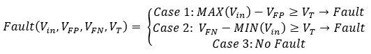
Based on the above equation the switch states are reflected in Table 2-2.
| Switch | State | Case | Equation |
|---|---|---|---|
| S1 | Opened | 2 | VFN - MIN(Vin) ≥ VT → 2V - 0.4V = 1.6V ≥ 0.7V |
| S2 | Opened | 2 | VFN - MIN(Vin) ≥ VT → 2V - 0.8V = 1.2V → 1.2V≥ 0.7V |
| S3 | Opened | 1 and 2 | VFN - MIN(Vin) ≥ VT → 2V - 1.2V = 0.8V → 0.8V ≥ 0.7V |
| MAX(Vin) - VFP ≥VT →45.2V - 44V = 1.2V →1.2V ≥ 0.7V | |||
| S4 | Closed | 3 | VFN - MIN(Vin) ≥ VT → 2V - 1.6V = 0.4V → 0.4V ≤ 0.7V |
| MAX(Vin) - VFP ≥VT →3.1V - 44V = -40.9V →-40.9V ≤0.7V |
During the ground shifting event the reference points of VIN1, VIN2, VIN3, VIN4, and the multiplexer will all be shifted to be greater than 0 V. This causes VIN1 and VIN2 to go below the reference potential of the switch – creating a fault condition and opening the switches S1 and S2. VIN3 not only violates the minimum voltage accepted into the channel protector, but also exceeds the maximum fault threshold causing the switch, S3, to either be opened due to over or under voltage. Finally, S4 is closed because the fault level + threshold was not met by VIN4 keeping the switch in a closed position and operating normally.
Next, the topic of miss-wiring. This is handled in very much the same was as the other fault protection features. Miss-wiring will often lead to too large of voltages on the incorrect pins. The previous fault protections still apply. If a miss-wiring creates an over or under voltage on one of the input pins and the signal is within the protection specs then TI’s Fault Protected Switches and Multiplexers will treat the miss-wiring as any other fault by detecting it and dealing with it by opening the switch or clamping the output or by keeping the switch high impedance when VDD is floating or 0V.
The final issue that was discussed in section one is that of latch-up events. These are prevented by using Latch-Up Immune Multiplexers and Switches – which TI’s Fault Protected Switches and Multiplexers are all Latch-Up Immune by Construction. In general, using buried oxide trench layers along with proper layout and guard rings latch up immunity is achieved by breaking the formation of the SCR with trenches and absorbing extra injected charge through guard rings or other similar structures. This means if a latch up causing event (injected current or voltage transient) is input to the Fault Protected Switch/Multiplexer the device will not latch up. This has two benefits – the first being that the VDD and VSS/GND pins will not be shorted as latch up will not happen and the second is that more sensitive parts are protected from latch up causing signals – as not every electronic component is built latch up immune. TI’s Fault Protected Switches and Multiplexers not only will prevent latch up, but since most latch up causing events are related to electrical overstress the fault protected multiplexer or switch can isolate the fault channel further preventing latch-up events down-stream from the input of the system.