SCEA065B November 2018 – March 2021 SN74AVC4T774 , SN74AXC1T45 , SN74AXC4T245 , SN74AXC4T774 , SN74AXC8T245 , SN74AXC8T245-Q1 , SN74AXCH1T45 , SN74AXCH4T245 , SN74AXCH8T245
2.4 Joint Test Action Group (JTAG)
Joint Test Action Group (JTAG) developed a hardware interface of the same name to allow debugging, testing, verification, and programming of embedded designs. JTAG usually operates using five lines: TCK, TMS, TDI, TDO, and TRST as listed in Table 2-2. Test Clock (TCK) provides the timing for the data input and output. Test Mode Select (TMS) allows the user to choose what will be tested. Test Data In (TDI) is where data to be tested is input to the device under test, the resulting output is carried on Test Data Out (TDO). The final signal, Test Reset (TRST), is optional and gives the ability to reset JTAG to the last known good state.
| SIGNAL | DESCRIPTION | DIRECTION |
|---|---|---|
| TCK | Test Clock Signal | Controller to Debugger |
| TDI | Test Data In | Controller to Debugger |
| TDO | Test Data Out | Debugger to Controller |
| TMS | Test Mode Select | Controller to Debugger |
| TRST | Test Reset | Controller to Debugger |
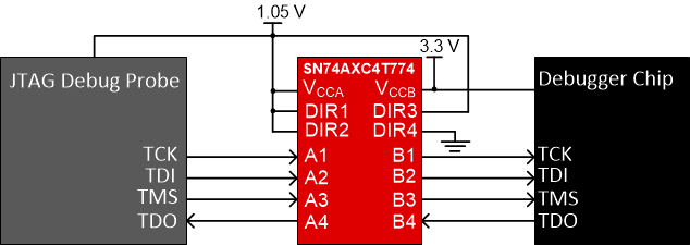
Since JTAG is similar to SPI, the configuration of voltage translators is similar. The key difference is that JTAG has four lines running in one direction and one in the opposite direction. To enable use of JTAG interface between a low voltage FPGA or processor, and a JTAG probe, the SN74AXC4T774 or the SN74AVC4T774 device, as configured in Figure 2-10 is recommended. Alternatively, one SN74AXC4T245 for the TCK, TMS, TDI, and TRST signal lines, and one SN74AXC1T45 for the TDO line operating in the other direction can be used, for the five-line JTAG interface.
 Figure 2-10 JTAG Voltage Translation Using SN74AXC4T774