SLAA929A December 2019 – March 2020 MSP430FR2353 , MSP430FR2355
Design Goals
| Input | Output | Supply | |||
|---|---|---|---|---|---|
| ViMin | ViMax | VoMin | VoMax | Vcc | Vee |
| 0.2 Vpp | 2 Vpp | 0.1 Vp | 1 Vp | 3.3 V | 0 V |
Design Description
Some MSP430™ microcontrollers (MCUs) contain configurable integrated signal chain elements such as op-amps, DACs, and programmable gain stages. These elements make up a peripheral called the Smart Analog Combo (SAC). For information on the different types of SACs and how to leverage their configurable analog signal chain capabilities, visit MSP430 MCUs Smart Analog Combo Training. To get started with your design, download the Half-Wave Rectifier Circuit Design Files.
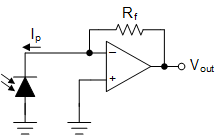
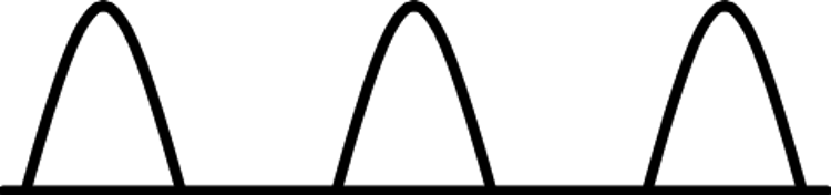
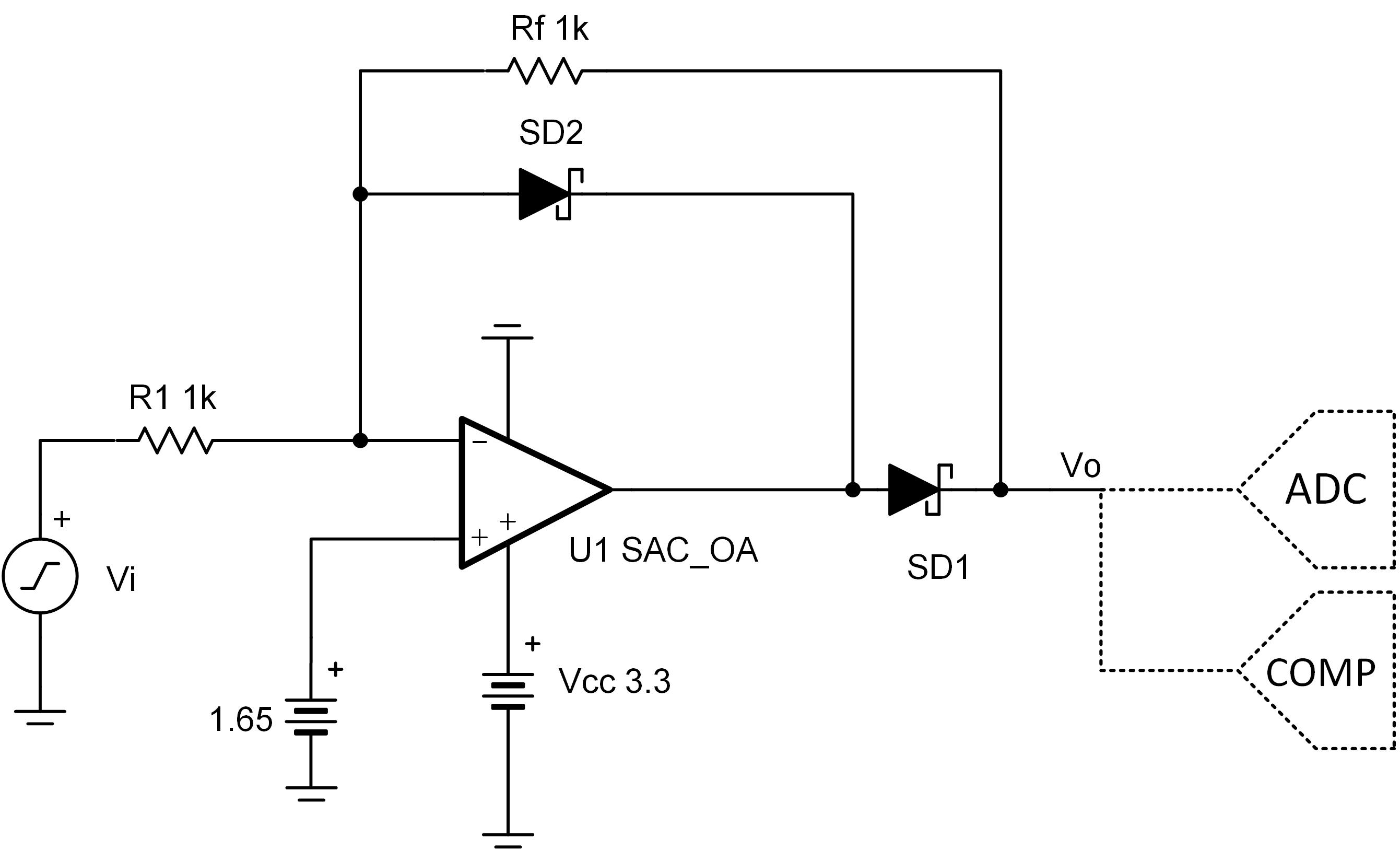
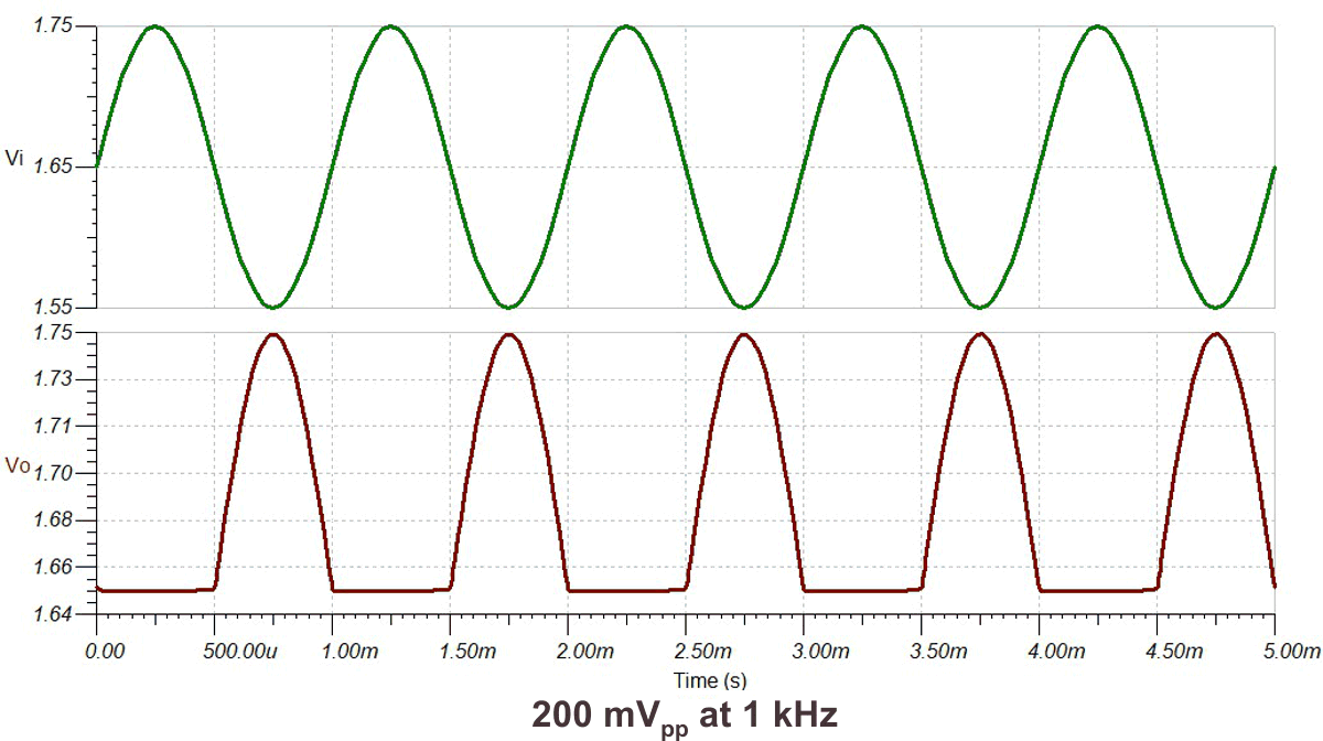
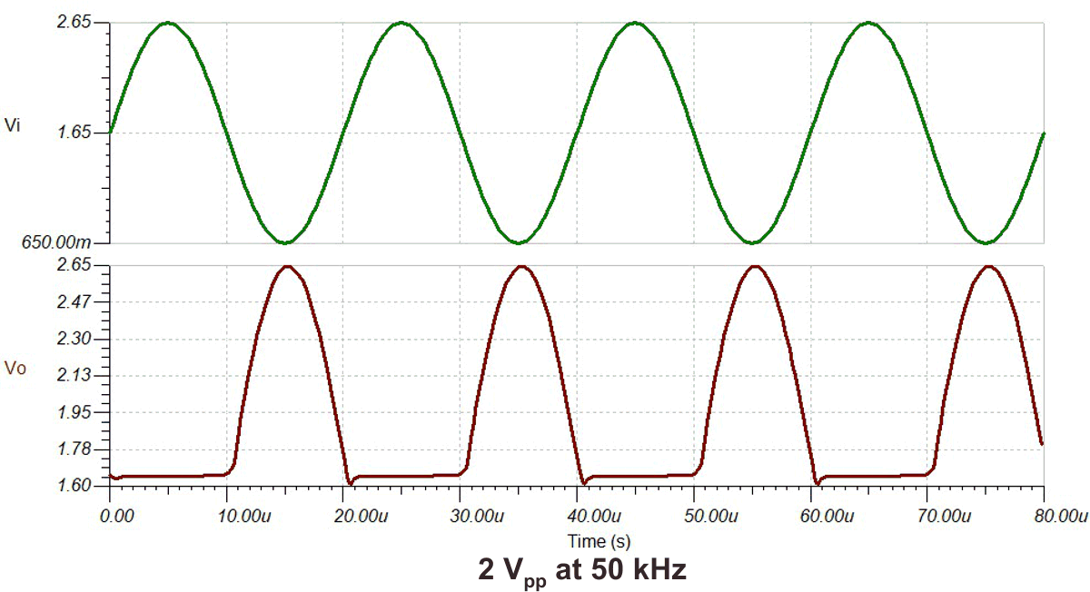
The precision half-wave rectifier inverts and transfers only the negative-half input of a time varying input signal (preferably sinusoidal) to its output. This circuit uses the MSP430FR2311 SAC_L1 op-amp in an inverting amplifier configuration with the appropriate diodes in place. There is room for further integration by using the integrated DAC in the MSP430FR2355 SAC_L3 block to provide the bias voltage on the non-inverting op-amp terminal. By appropriately selecting the feedback resistor values, different gains can be achieved. Precision half-wave rectifiers are commonly used with other op amp circuits such as a peak-detector or bandwidth limited non-inverting amplifier to produce a DC output voltage. The output of the SAC_L3 op-amp can be cascaded with the other 3 SAC_L3 blocks in the MSP430FR2355 to expand upon the analog signal chain functionality or sampled directly by the onboard ADC or monitored by the onboard comparator for further processing inside the MCU. This configuration has been designed to work for sinusoidal input signals between 0.2 Vpp and 2 Vpp at frequencies up to 50 kHz.
Design Notes
- Set output range based on linear output swing (see Aol specification).
- Use fast switching diodes. High-frequency input signals will be distorted depending on the speed by which the diodes can transition from blocking to forward conducting mode. Schottky diodes might be a preferable choice, since these have faster transitions than pn-junction diodes at the expense of higher reverse leakage.
- The resistor tolerance sets the circuit gain error.
- Minimize noise errors by selecting low-value resistors.
- If the solution is implemented using the MSP430FR2311, the circuit can be realized by the SAC_L1 op-amp in general purpose mode or the Transimpedance Amplifier (TIA). In both cases the bias voltage can be set using a resistor divider or external DAC.
- If the TIA op-amp is used, the input voltage would need to be kept below VCC/2 to operate within the peripheral's common-mode input specifications.
- If the solution is implemented using the MSP430FR2355, the circuit can be realized using any of the 4 on-board SAC_L3 peripherals in DAC mode in order to generate the bias voltage on the non-inverting op-amp terminal.
- When the input signal changes polarities, the amplifier output must slew two diode voltage drops. The MSP430 SAC and TIA op-amps can be configured in "High-Speed Mode" to achieve a higher slew rate.
- The Half-Wave Rectifier Circuit Design Files include code examples showing how to properly initialize the SAC peripherals.
Design Steps
- Set the desired gain of the half-wave rectifier to select the feedback resistors.
- Where Req is the parallel combination of R1 and Rf
- Select the resistors such that the resistor noise is negligible compared to the voltage broadband noise of the op amp.
Design Simulations
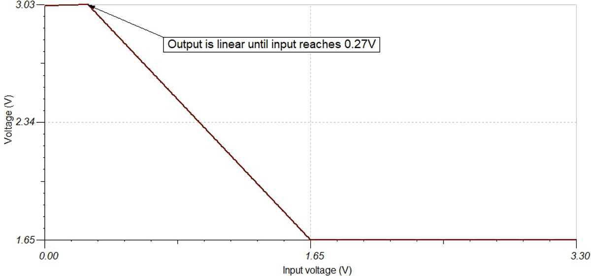
DC Simulation Results
Transient Simulation Results
Target Applications
References
- MSP430 Half-Wave Rectifier Circuit Code Examples and SPICE Simulation File
- Analog Engineer's Circuit Cookbooks
- MSP430FR2311 TINA-TI Spice Model
- MSP430 MCUs Smart Analog Combo Training
Design Featured Op Amp
| MSP430FRxx Smart Analog Combo | ||
|---|---|---|
| MSP430FR2311 SAC_L1 | MSP430FR2355 SAC_L3 | |
| Vcc | 2.0 V to 3.6 V | |
| VCM | -0.1 V to VCC + 0.1 V | |
| Vout | Rail-to-rail | |
| Vos | ±5 mV | |
| AOL | 100 dB | |
| Iq | 350 µA (high-speed mode) | |
| 120 µA (low-power mode) | ||
| Ib | 50 pA | |
| UGBW | 4 MHz (high-speed mode) | 2.8 MHz (high-speed mode) |
| 1.4 MHz (low-power mode) | 1 MHz (low-power mode) | |
| SR | 3 V/µs (high-speed mode) | |
| 1 V/µs (low-power mode) | ||
| Number of channels | 1 | 4 |
| http://www.ti.com/product/MSP430FR2311 | ||
| http://www.ti.com/product/MSP430FR2355 | ||
Design Alternate Op Amp
| MSP430FR2311 Transimpedance Amplifier | |
|---|---|
| Vcc | 2.0 V to 3.6 V |
| VCM | -0.1 V to VCC/2 V |
| Vout | Rail-to-rail |
| Vos | ±5 mV |
| AOL | 100 dB |
| Iq | 350 µA (high-speed mode) |
| 120 µA (low-power mode) | |
| Ib | 5 pA (TSSOP-16 with OA-dedicated pin input) |
| 50 pA (TSSOP-20 and VQFN-16) | |
| UGBW | 5 MHz (high-speed mode) |
| 1.8 MHz (low-power mode) | |
| SR | 4 V/µs (high-speed mode) |
| 1 V/µs (low-power mode) | |
| Number of channels | 1 |
| http://www.ti.com/product/MSP430FR2311 | |
Related MSP430 Circuits