SLAA988A December 2020 – January 2022 TAS2563
1.2 VBAT
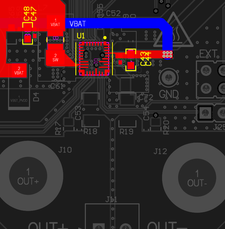
VBAT is the battery power supply input. It carries a considerable amount of current when the internal boost is used. VBAT trace can be separated in two, one trace that supplies the boost inductor (high current) and another trace that supplies the VBAT pin from the device (low current). Each termination of the VBAT supply must be decoupled thus decoupling capcaitors must be placed next to both the boost inductor and the VBAT pin from the IC.
At least a 0.1uF and 10uF must be used to bypass VBAT to GND close to the boost inductor, and at leat a 1uF must be used to bypass VBAT to GND close to the VBAT pin from the IC.
It is important to consider the following recommendations for VBAT:
Include additional bulk capacitors to reduce overall THD+N at high power, most important hen using low VBAT voltage levels.
Use wide traces for VBAT to handle the total output power.
Do not use vias between the devie pin, inductor terminal and related capacitors.
 Figure 1-4 VBAT Connection