SLAAED5A June 2023 – September 2025 AFE11612-SEP , OPA4H199-SEP
- 1
- Abstract
- Trademarks
- 1 LDMOS and GaN Power Amplifier FET PA Basics
- 2 VGS Compensation
- 3 Sequencing
- 4 An Integrated PA Biasing Solution
- 5 Negative Biasing for GaN PAs
- 6 Fast Switching for TDD Applications
- 7 VDRAIN Switching Circuit
- 8 Controlled Gate-Sequencing Circuit
- 9 VDRAIN Monitoring
- 10External Negative Power Supply Monitoring
- 11PA Temperature Monitoring
- 12Summary
- 13References
- 14Revision History
1 LDMOS and GaN Power Amplifier FET PA Basics
Most radio frequency (RF) antenna systems feature power amplifiers (PA) for their RF transmitter design. Many aerospace and space applications include antenna systems, such as:
PA biasing circuits are implemented in RF antenna systems to ensure two things. First, that the power output of the amplifier is known and controlled, and second, that the system is powered on and off safely to reduce the risk of damaging the PA. PAs are commonly designed with gallium nitride (GaN), gallium arsenide (GaAs), or laterally diffused MOSFET (LDMOS) transistors. Power output in both GaN and LDMOS FETs (field-effect transistors) is dependent on the current that flows through the device from the drain to the source (IDS).
 Figure 1-1 GaN and LDMOS FETs
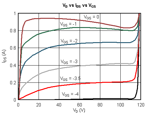
IDS is determined by a few variables: the drain voltage (VDRAIN), the gate voltage (VGS), and temperature. Figure 1-2 shows an example of IDS values against the VDRAIN for a selection of VGS voltages for a GaN PA. The higher VGS voltages result in a higher IDS, or more power from the amplifier. When VGS is sufficiently low, the PA allows virtually zero IDS current. This VGS voltage is called the pinch-off voltage. IDS is also dependent on the VDRAIN, but most designers do not vary the VDRAIN. Instead, designers use optimized VDRAIN voltages for the desired power levels. The VDRAIN values are usually about 50 V for GaN PAs and 28 V for LDMOS PAs.
 Figure 1-2 FET VDRAIN, IDS, and VGS Behavior