SLAU320AJ July   2010  – May 2021


  1.   Trademarks
  2. 1Introduction
    1. 1.1 About This Document
    2. 1.2 Organization of This Document
  3. 2Programming Using the JTAG Interface
    1. 2.1 Introduction
      1. 2.1.1 MSP430 JTAG Restrictions (Noncompliance With IEEE Std 1149.1)
      2. 2.1.2 TAP Controller State Machine
    2. 2.2 Interface and Instructions
      1. 2.2.1 JTAG Interface Signals
        1. 2.2.1.1 Pros and Cons of 2-Wire Spy-Bi-Wire and 4-Wire JTAG
        2. 2.2.1.2 4-Wire JTAG Interface
        3. 2.2.1.3 2-Wire Spy-Bi-Wire (SBW) JTAG Interface
      2. 2.2.2 JTAG Access Macros
        1. 2.2.2.1 Macros for 4-Wire JTAG Interface
          1. 2.2.2.1.1 IR_SHIFT (8-Bit Instruction)
          2. 2.2.2.1.2 DR_SHIFT16 (16-Bit Data)
          3. 2.2.2.1.3 DR_SHIFT20 (20-Bit Address) (Applies Only to MSP430X Devices)
          4. 2.2.2.1.4 MsDelay (Time)
          5. 2.2.2.1.5 SetTCLK
          6. 2.2.2.1.6 ClrTCLK
        2. 2.2.2.2 Macros for Spy-Bi-Wire (SBW) Interface
      3. 2.2.3 Spy-Bi-Wire (SBW) Timing and Control
        1. 2.2.3.1 Basic Timing
        2. 2.2.3.2 TMS Slot
          1. 2.2.3.2.1 TMSH Macro
          2. 2.2.3.2.2 TMSL Macro
          3. 2.2.3.2.3 TMSLDH Macro
        3. 2.2.3.3 TDI Slot
          1. 2.2.3.3.1 TDIH Macro
          2. 2.2.3.3.2 TDIL Macro
        4. 2.2.3.4 TDO Slot
          1. 2.2.3.4.1 TDO_RD Macro
          2. 2.2.3.4.2 TDOsbw Macro (No Read)
        5. 2.2.3.5 TCLK Handling in Spy-Bi-Wire (SBW) Mode
          1. 2.2.3.5.1 SetTCLK and ClrTCLK
          2. 2.2.3.5.2 TCLK Strobes
      4. 2.2.4 JTAG Communication Instructions
        1. 2.2.4.1 Controlling the Memory Address Bus (MAB)
          1. 2.2.4.1.1 IR_ADDR_16BIT
          2. 2.2.4.1.2 IR_ADDR_CAPTURE
        2. 2.2.4.2 Controlling the Memory Data Bus (MDB)
          1. 2.2.4.2.1 IR_DATA_TO_ADDR
          2. 2.2.4.2.2 IR_DATA_16BIT
          3. 2.2.4.2.3 IR_DATA_QUICK
          4. 2.2.4.2.4 IR_BYPASS
        3. 2.2.4.3 Controlling the CPU
          1. 2.2.4.3.1 IR_CNTRL_SIG_16BIT
          2. 2.2.4.3.2 IR_CNTRL_SIG_CAPTURE
          3. 2.2.4.3.3 IR_CNTRL_SIG_RELEASE
        4. 2.2.4.4 Memory Verification by Pseudo Signature Analysis (PSA)
          1. 2.2.4.4.1 IR_DATA_PSA
          2. 2.2.4.4.2 IR_SHIFT_OUT_PSA
        5. 2.2.4.5 JTAG Access Security Fuse Programming
          1. 2.2.4.5.1 IR_PREPARE_BLOW
          2. 2.2.4.5.2 IR_EX_BLOW
    3. 2.3 Memory Programming Control Sequences
      1. 2.3.1 Start-Up
        1. 2.3.1.1 Enable JTAG Access
        2. 2.3.1.2 Fuse Check and Reset of the JTAG State Machine (TAP Controller)
      2. 2.3.2 General Device (CPU) Control Functions
        1. 2.3.2.1 Function Reference for 1xx, 2xx, 4xx Families
          1. 2.3.2.1.1 Taking the CPU Under JTAG Control
          2. 2.3.2.1.2 Set CPU to Instruction-Fetch
          3. 2.3.2.1.3 Setting the Target CPU Program Counter (PC)
          4. 2.3.2.1.4 Controlled Stop or Start of the Target CPU
          5. 2.3.2.1.5 Resetting the CPU While Under JTAG Control
          6. 2.3.2.1.6 Release Device From JTAG Control
        2. 2.3.2.2 Function Reference for 5xx and 6xx Families
          1. 2.3.2.2.1 Taking the CPU Under JTAG Control
          2. 2.3.2.2.2 Setting the Target CPU Program Counter (PC)
          3. 2.3.2.2.3 Resetting the CPU While Under JTAG Control
          4. 2.3.2.2.4 Release Device From JTAG Control
          5. 2.3.2.2.5 74
      3. 2.3.3 Accessing Non-Flash Memory Locations With JTAG
        1. 2.3.3.1 Read Access
        2. 2.3.3.2 Write Access
        3. 2.3.3.3 Quick Access of Memory Arrays
          1. 2.3.3.3.1 Flow for Quick Read (All Memory Locations)
          2. 2.3.3.3.2 Flow for Quick Write
      4. 2.3.4 Programming the Flash Memory (Using the Onboard Flash Controller)
        1. 2.3.4.1 Function Reference for 1xx, 2xx, 4xx Families
        2. 2.3.4.2 Function Reference for 5xx and 6xx Families
      5. 2.3.5 Erasing the Flash Memory (Using the Onboard Flash Controller)
        1. 2.3.5.1 Function Reference for 1xx, 2xx, 4xx Families
          1. 2.3.5.1.1 Flow to Erase a Flash Memory Segment
          2. 2.3.5.1.2 Flow to Erase the Entire Flash Address Space (Mass Erase)
        2. 2.3.5.2 Function Reference for 5xx and 6xx Families
      6. 2.3.6 Reading From Flash Memory
      7. 2.3.7 Verifying the Target Memory
      8. 2.3.8 FRAM Memory Technology
        1. 2.3.8.1 Writing and Reading FRAM
        2. 2.3.8.2 Erasing FRAM
    4. 2.4 JTAG Access Protection
      1. 2.4.1 Burning the JTAG Fuse - Function Reference for 1xx, 2xx, 4xx Families
        1. 2.4.1.1 Standard 4-Wire JTAG
          1. 2.4.1.1.1 Fuse-Programming Voltage on TDI Pin (Dedicated JTAG Pin Devices Only)
          2. 2.4.1.1.2 Fuse-Programming Voltage On TEST Pin
        2. 2.4.1.2 Fuse-Programming Voltage Using SBW
      2. 2.4.2 Programming the JTAG Lock Key - Function Reference for 5xx, 6xx, and FRxx Families
        1. 2.4.2.1 Flash Memory Devices
        2. 2.4.2.2 FRAM Memory Devices
      3. 2.4.3 Testing for a Successfully Protected Device
      4. 2.4.4 Unlocking an FRAM Device in Protected and Secured Modes
        1. 2.4.4.1 FR5xx and FR6xx Devices
        2. 2.4.4.2 FR4xx and FR2xx Devices
      5. 2.4.5 Memory Protection Unit Handling
      6. 2.4.6 Intellectual Property Encapsulation (IPE)
      7. 2.4.7 FRAM Write Protection
    5. 2.5 JTAG Function Prototypes
      1. 2.5.1 Low-Level JTAG Functions
      2. 2.5.2 High-Level JTAG Routines
    6. 2.6 JTAG Features Across Device Families
    7. 2.7 References
  4. 3JTAG Programming Hardware and Software Implementation
    1. 3.1 Implementation History
    2. 3.2 Implementation Overview
    3. 3.3 Software Operation
    4. 3.4 Software Structure
      1. 3.4.1 Programmer Firmware
      2. 3.4.2 Target Code
        1. 3.4.2.1 Target Code Download for Replicator430, Replicator430X, and Replicator430Xv2
        2. 3.4.2.2 Target Code Download for Replicator430FR (FRAM)
    5. 3.5 Hardware Setup
      1. 3.5.1 Host Controller
      2. 3.5.2 Target Connection
      3. 3.5.3 Host Controller or Programmer Power Supply
      4. 3.5.4 Third-Party Support
  5. 4Errata and Revision Information
    1. 4.1 Known Issues
    2. 4.2 Revisions and Errata From Previous Documents
  6. 5Revision History

2-Wire Spy-Bi-Wire (SBW) JTAG Interface

The core JTAG logic integrated into devices that support 2-wire mode is identical to 4-wire-only devices. The fundamental difference is that 2-wire devices implement additional logic that is used to convert the 2-wire communication into the standard 4-wire communication internally. In this way, the existing JTAG emulation methodology of the MSP430 can be fully used.
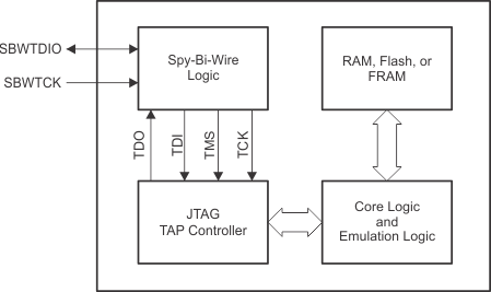
GUID-E2FB5CBB-714B-4C69-9249-FC69A930A949-low.gifFigure 2-2 Spy-Bi-Wire Basic Concept

The 2-wire interface is made up of the SBWTCK (Spy-Bi-Wire test clock) and SBWTDIO (Spy-Bi-Wire test data input/output) pins. The SBWTCK signal is the clock signal and is a dedicated pin. In normal operation, this pin is internally pulled to ground. The SBWTDIO signal represents the data and is a bidirectional connection. To reduce the overhead of the 2-wire interface, the SBWTDIO line is shared with the RST/NMI pin of the device.

Section 2.6 describes the MSP430 devices and their respective JTAG interface implementation.