SLAU678C March   2016  – November 2022


  1.   Abstract
  2.   Trademarks
  3. 1Getting Started
    1. 1.1 Introduction
    2. 1.2 Key Features
    3. 1.3 What's Included
      1. 1.3.1 Kit Contents
      2. 1.3.2 Software Examples
    4. 1.4 First Steps: Out-of-Box Experience
      1. 1.4.1 Connecting to the Computer
      2. 1.4.2 Running the Out-of-Box Demo
        1. 1.4.2.1 Live Temperature Mode
        2. 1.4.2.2 FRAM Data Log Mode
        3. 1.4.2.3 SD Card Data Log Mode
    5. 1.5 Next Steps: Looking Into the Provided Code
  4. 2Hardware
    1. 2.1 Block Diagram
    2. 2.2 Hardware Features
      1. 2.2.1 MSP430FR5994 MCU
      2. 2.2.2 eZ-FET Onboard Debug Probe With EnergyTrace++ Technology
      3. 2.2.3 Debug Probe Connection: Isolation Jumper Block
      4. 2.2.4 Application (or Backchannel) UART
      5. 2.2.5 Special Features
        1. 2.2.5.1 microSD Card
        2. 2.2.5.2 220-mF Super Capacitor
    3. 2.3 Power
      1. 2.3.1 eZ-FET USB Power
      2. 2.3.2 BoosterPack Plug-in Module and External Power Supply
      3. 2.3.3 Super Cap (C1)
        1. 2.3.3.1 Charging the Super Cap
        2. 2.3.3.2 Using the Super Cap
        3. 2.3.3.3 Disabling the Super Cap
    4. 2.4 Measure MSP430 Current Draw
    5. 2.5 Clocking
    6. 2.6 Using the eZ-FET Debug Probe With a Different Target
    7. 2.7 BoosterPack Plug-in Module Pinout
    8. 2.8 Design Files
      1. 2.8.1 Hardware
      2. 2.8.2 Software
    9. 2.9 Hardware Change Log
  5. 3Software Examples
    1. 3.1 Out-of-Box Software Example
      1. 3.1.1 Source File Structure
      2. 3.1.2 Out-of-Box Demo GUI
      3. 3.1.3 Power Up and Idle
      4. 3.1.4 Live Temperature Mode
      5. 3.1.5 FRAM Log Mode
      6. 3.1.6 SD Card Log Mode
    2. 3.2 Blink LED Example
      1. 3.2.1 Source File Structure
    3. 3.3 BOOSTXL-AUDIO Audio Record and Playback Example
      1. 3.3.1 Source File Structure
      2. 3.3.2 Operation
    4. 3.4 Filtering and Signal Processing With LEA Reference Design Example
      1. 3.4.1 Source File Structure
      2. 3.4.2 Operation
    5. 3.5 Emulating EEPROM Reference Design Example
      1. 3.5.1 Source File Structure
      2. 3.5.2 Operation
  6. 4Resources
    1. 4.1 Integrated Development Environments
      1. 4.1.1 TI Cloud Development Tools
        1. 4.1.1.1 TI Resource Explorer Cloud
        2. 4.1.1.2 Code Composer Studio Cloud
      2. 4.1.2 Code Composer Studio™ IDE
      3. 4.1.3 IAR Embedded Workbench for MSP430
    2. 4.2 LaunchPad Websites
    3. 4.3 MSPWare and TI Resource Explorer
    4. 4.4 FRAM Utilities
      1. 4.4.1 Compute Through Power Loss (CTPL)
    5. 4.5 MSP430FR5994 MCU
      1. 4.5.1 Device Documentation
      2. 4.5.2 MSP430FR5994 Code Examples
      3. 4.5.3 MSP430 Application Notes and TI Reference Designs
    6. 4.6 Community Resources
      1. 4.6.1 TI E2E Support Forums
      2. 4.6.2 Community at Large
  7. 5FAQ
  8. 6Schematics
  9. 7Revision History

MSP430FR5994 MCU

The MSP430FR5994 is the next device in TI's new ULP FRAM technology platform. FRAM is a cutting-edge memory technology that combines the best features of flash and RAM into one nonvolatile memory. For more information on FRAM, see www.ti.com/fram.

Device features include:

  • 1.8-V to 3.6-V operation
  • 16-bit RISC architecture up to 16-MHz system clock and 8-MHz FRAM access
  • 256KB of FRAM and 8KB of SRAM
  • 16-channel 12-bit ADC
  • 16-channel analog comparator
  • Six 16-bit timers with seven capture/compare registers each
  • 6-channel direct memory access (DMA)
  • 128-bit or 256-bit AES
  • 32-bit hardware multiplier (MPY)
  • 68 GPIOs

Figure 2-3 shows the pinout of the MSP430FR5994 MCU in the 80-pin PN package.
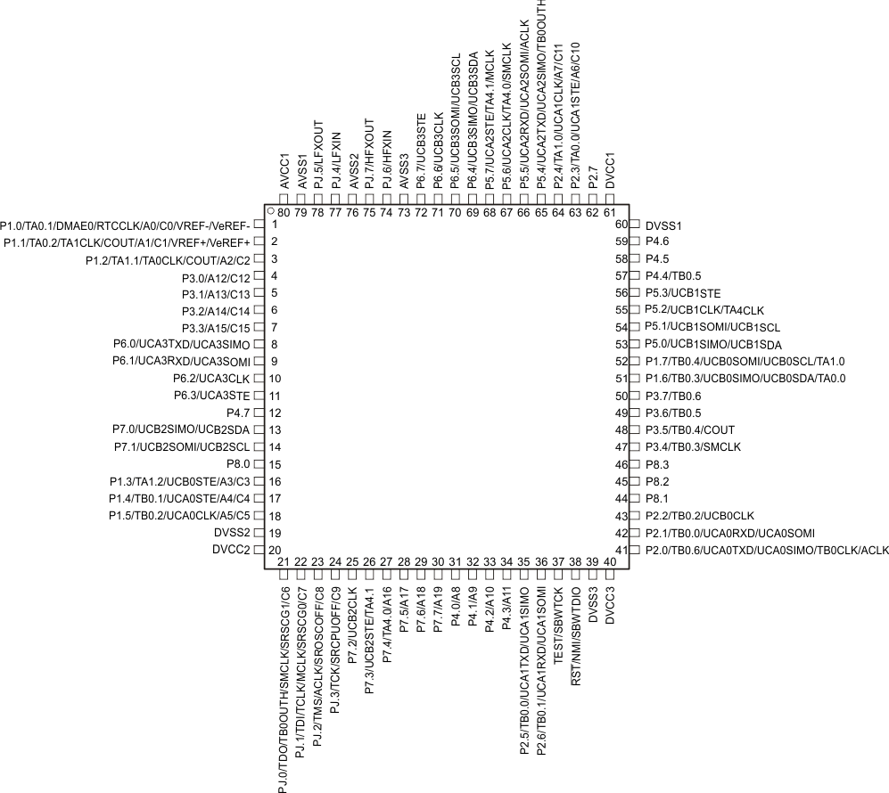
GUID-960A9942-4DB9-40FF-8ECC-4DA692F66D4E-low.gif Figure 2-3 MSP430FR5994 Pinout