SLLA539B November 2020 – December 2021 TCAN1051-Q1 , TCAN1051G-Q1 , TCAN1051GV-Q1 , TCAN1051H-Q1 , TCAN1051HG-Q1 , TCAN1051HGV-Q1 , TCAN1051HV-Q1 , TCAN1051V-Q1
4.1 SOIC and VSON Packages
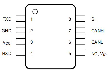
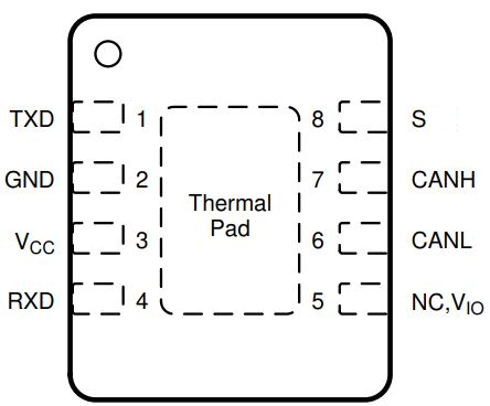
Figure 4-1 shows the TCAN1051-Q1/TCAN1051V-Q1 SOIC pin diagram. Figure 4-2 shows the TCAN1051-Q1/TCAN1051V-Q1 VSON pin diagram. For a detailed description of the device pins please refer to the Pin Configurations and Functions section in the TCAN1051-Q1/TCAN1051V-Q1 data sheet.
 Figure 4-1 SOIC Pin Diagram
  Figure 4-2 VSON Pin Diagram
Table 4-2 Pin FMA for Device Pins
Short-Circuited to Ground
| Pin Name | Pin No. | Description of Potential Failure Effect(s) | Failure Effect Class |
|---|---|---|---|
| TXD | 1 | Device will enter dominant time out mode. Unable to transmit data. | B |
| GND | 2 | None | D |
| VCC | 3 | Device unpowered, high ICC current. | B |
| RXD | 4 | Transceiver output biased dominant, unable to receive data from the CAN bus. Internal damage possible. | A |
| NC | 5 | None | D |
| VIO | 5 | Device will be in protected mode. Transceiver passive on bus. | B |
| CANL | 6 | VO(REC) spec violated. Degraded EMC performance. | C |
| CANH | 7 | Device cannot drive dominant to the bus, no communication possible. | B |
| S | 8 | S biased low, transceiver unable to enter silent mode. | B |
| Thermal Pad | - | None | D |
Note: The VSON package includes
a thermal pad.
Table 4-3 Pin FMA for Device Pins
Open-Circuited
| Pin Name | Pin No. | Description of Potential Failure Effect(s) | Failure Effect Class |
|---|---|---|---|
| TXD | 1 | TXD pin defaults recessive, device always recessive and unable to transmit data. | B |
| GND | 2 | Device unpowered. | B |
| VCC | 3 | Device unpowered. | B |
| RXD | 4 | No RXD output, unable to receive data. | B |
| NC | 5 | None | D |
| VIO | 5 | Device will be in protected mode. Transceiver passive on bus. | B |
| CANL | 6 | Device cannot drive dominant on the bus, unable to communicate. | B |
| CANH | 7 | Device cannot drive dominant on the bus, unable to communicate. | B |
| S | 8 | S pin defaults high, transceiver stuck in silent mode. | B |
| Thermal Pad | - | None | D |
Note: The VSON package includes a
thermal pad.
Table 4-4 Pin FMA for Device Pins
Short-Circuited to Adjacent Pin
| Pin Name | Pin No. | Shorted to | Description of Potential Failure Effect(s) | Failure Effect Class |
|---|---|---|---|---|
| TXD | 1 | GND | Device will enter dominant time out mode. Unable to transmit data. | B |
| GND | 2 | VCC | Device unpowered, high ICC current. | B |
| VCC | 3 | RXD | RXD output biased recessive, unable to receive data. | B |
| NC | 5 | CANL | None | D |
| VIO | 5 | CANL | Bus biased recessive, no communication possible. IOS current may be reached on CANL. | B |
| CANL | 6 | CANH | Bus biased recessive, no communication possible. IOS current may be reached on CANH/CANL. | B |
| CANH | 7 | S | Driver turns off when a dominant is driven. May not enter normal mode. | B |
Note: The VSON package includes a
thermal pad. All device pins are adjacent to the thermal pad. The device behavior
when pins are shorted to the thermal pad depends on which net is connected to the
thermal pad.
Table 4-5 Pin FMA for Device Pins
Short-Circuited to VCC
| Pin Name | Pin No. | Description of Potential Failure Effect(s) | Failure Effect Class |
|---|---|---|---|
| TXD | 1 | TXD biased recessive, unable to transmit data. | B |
| GND | 2 | Device unpowered, high ICC current. | B |
| VCC | 3 | None | D |
| RXD | 4 | RXD pin biased recessive, unable to receive data. | B |
| NC | 5 | None | D |
| VIO | 5 | IO pins will operate as 5V input/outputs. Microcontroller may be damaged if VCC > VIO. | C |
| CANL | 6 | RXD always recessive, no communication possible. IOS current may be reached. | B |
| CANH | 7 | VO(REC) spec violated, degraded EMC performance. | C |
| S | 8 | S biased high, transceiver always in silent mode. | B |
Table 4-6 Pin FMA for Device Pins Short-Circuited to
VBAT
| Pin Name | Pin No. | Description of Potential Failure Effect(s) | Failure Effect Class |
|---|---|---|---|
| TXD | 1 | Absolute maximum violation, transceiver may be damaged. Unable to transmit data. | A |
| GND | 2 | Device unpowered, high IBATcurrent | B |
| VCC | 3 | Absolute maximum violation, transceiver may be damaged. Bus may be unable to communicate. | A |
| RXD | 4 | Absolute maximum violation, transceiver may be damaged. Unable to receive data. | A |
| NC | 5 | None | D |
| VIO | 5 | Absolute maximum violation, transceiver may be damaged. | A |
| CANL | 6 | RXD always recessive, no communication possible. IOScurrent may be reached. | B |
| CANH | 7 | VO(REC) spec violated, degraded EMC performance. | C |
| S | 8 | Absolute maximum violation, transceiver may be damaged. Transceiver stuck in silent mode. | A |
Table 4-7 Pin FMA for Device Pins Short-Circuited to VIO
| Pin Name | Pin No. | Description of Potential Failure Effect(s) | Failure Effect Class |
|---|---|---|---|
| TXD | 1 | TXD biased recessive indefinitely, unable to transmit data. | B |
| GND | 2 | Device unpowered, high IIO current. | B |
| VCC | 3 | IO pins will operate as 5V input/outputs. Microcontroller may be damaged if VCC > VIO. | C |
| RXD | 4 | RXD pin biased recessive indefinitely, unable to receive data. | B |
| NC | 5 | None | D |
| VIO | 5 | None | D |
| CANL | 6 | RXD always recessive, no communication possible. IOS current may be reached if VIO ≥ 3.3V. | B |
| CANH | 7 | VO(REC) spec violated if, degraded EMC performance. | C |
| S | 8 | S biased high indefinitely, transceiver always in silent mode. | B |