SLLSEL2C September 2015 – July 2016 SN65DP149 , SN75DP149
PRODUCTION DATA.
- 1 Features
- 2 Applications
- 3 Description
- 4 Revision History
- 5 Description (continued)
- 6 Pin Configuration and Functions
-
7 Specifications
- 7.1 Absolute Maximum Ratings
- 7.2 ESD Ratings
- 7.3 Recommended Operating Conditions
- 7.4 Thermal Information
- 7.5 Power Supply Electrical Characteristics
- 7.6 Differential Input Electrical Characteristics
- 7.7 HDMI and DVI TMDS Output Electrical Characteristics
- 7.8 DDC, and I2C Electrical Characteristics
- 7.9 HPD Electrical Characteristics
- 7.10 HDMI and DVI Main Link Switching Characteristics
- 7.11 HPD Switching Characteristics
- 7.12 DDC and I2C Switching Characteristics
- 7.13 Parameter Measurement Information
- 7.14 Typical Characteristics
- 8 Detailed Description
- 9 Application and Implementation
- 10Power Supply Recommendations
- 11Layout
- 12Device and Documentation Support
- 13Mechanical, Packaging, and Orderable Information
7 Specifications
7.1 Absolute Maximum Ratings
over operating free-air temperature (unless otherwise noted) (1)(2)| MIN | MAX | UNIT | ||
|---|---|---|---|---|
| Supply voltage(3) | VCC | –0.3 | 4 | V |
| VDD | –0.3 | 1.4 | V | |
| Voltage | Main link input (IN_Dx AC-coupled mode) | 1.56 | V | |
| TMDS outputs ( OUT_Dx) | –0.3 | 4 | V | |
| HPD_SRC, Vsadj, SDA_CTL, SCL_CTL, OE, HDMI_SEL/A1, EQ_SEL/A0, I2C_EN/PIN, SLEW_CTL, SDA_SRC, SCL_SRC | –0.3 | 4 | V | |
| HPD_SNK, SDA_SNK, SCL_SNK | –0.3 | 6 | V | |
| Continuous power dissipation | See Thermal Information | |||
| Storage temperature, Tstg | –65 | 150 | °C | |
(1) Stresses beyond those listed under Absolute Maximum Ratings may cause permanent damage to the device. These are stress ratings only and functional operation of the device at these or any conditions beyond those indicated under Recommended Operating Conditions is not implied. Exposure to absolute-maximum-rated conditions for extended periods may affect device reliability.
(2) All voltage values, except differential voltages, are with respect to network ground terminal.
(3) Tested in accordance with JEDEC Standard 22, Test Method A114-B.
7.2 ESD Ratings
| VALUE | UNIT | |||
|---|---|---|---|---|
| V(ESD) | Electrostatic discharge | Human body model (HBM), per ANSI/ESDA/JEDEC JS-001, all pins(1) | ±2000 | V |
| Charged device model (CDM), per JEDEC specification JESD22-C101, all pins(2) | ±500 | V | ||
(1) JEDEC document JEP155 states that 500-V HBM allows safe manufacturing with a standard ESD control process.
(2) JEDEC document JEP157 states that 250-V CDM allows safe manufacturing with a standard ESD control process.
7.3 Recommended Operating Conditions
over operating free-air temperature range (unless otherwise noted)| MIN | NOM | MAX | UNIT | |||
|---|---|---|---|---|---|---|
| GENERAL PARAMETERS | ||||||
| VCC | Supply voltage | 3 | 3.3 | 3.6 | V | |
| VDD | 1.00 | 1.1 | 1.27 | |||
| TCASE | Case temperature for RSB package | 93.5 | °C | |||
| TA | Operating free-air temperature | SN75DP149 | 0 | 85 | °C | |
| SN65DP149 | –40 | 85 | ||||
| MAIN LINK DIFFERENTIAL PINS | ||||||
| VID_PP | Peak-to-peak input differential voltage | 75 | 1200 | mv | ||
| VIC | Input common mode voltage | 0 | 2 | V | ||
| CAC | AC coupling capacitance | 75 | 100 | 200 | nF | |
| dR | Data rate | 0.25 | 5 | Gbps | ||
| Vsadj | TMDS-compliant swing voltage bias resistor | 6.5 | kΩ | |||
| CONTROL PINS | ||||||
| VI-DC | DC input voltage | –0.3 | 3.6 | V | ||
| VIL(1) | Low-level input voltage at OE | 0.8 | V | |||
| Low-level input voltage at SLEW_CTL, PRE_SEL, EQ_SEL/A0, SWAP/POL | 0.3 | |||||
| VIM(1) | No connect input voltage at SLEW_CTL, PRE_SEL, EQ_SEL/A0, SWAP/POL | 1 | 1.2 | 1.4 | V | |
| VIH(1) | High-level input voltage at SLEW_CTL, OE(2) , PRE_SEL, EQ_SEL/A0, SWAP/POL | 2.6 | V | |||
| VOL | Low-level output voltage | 0.4 | V | |||
| VOH | High-level output voltage | 2.4 | V | |||
| IIH | High-level input current | –30 | 30 | µA | ||
| IIL | Low-level input current | –10 | 10 | µA | ||
| IOS | Short circuit output current | –50 | 50 | mA | ||
| IOZ | High impedance output current | 10 | µA | |||
| ROEPU | Pullup resistance on OE pin | 150 | 250 | kΩ | ||
(1) These values are based upon a microcontroller driving the control pins. The pullup/pulldown/floating resistor configuration will set the internal bias to the proper voltage level which will not match the values shown here.
(2) This value is based upon a microcontroller driving the OE pin. A passive reset circuit using an external capacitor and the internal pullup resistor will set OE pin properly, but may have a different value than shown due to internal biasing.
7.4 Thermal Information
over operating free-air temperature range (unless otherwise noted)| THERMAL METRIC(1) | SNx5DP149 | UNIT | |
|---|---|---|---|
| RSB (WQFN) | |||
| 40 PINS | |||
| RθJA | Junction-to-ambient thermal resistance | 37.3 | °C/W |
| RθJB | Junction-to-board thermal resistance (High-K board(2)) | 9.9 | °C/W |
| RθJC(top) | Junction-to-case (top) thermal resistance (High-K board(2)) | 23.1 | °C/W |
| RθJC(bot) | Junction-to-case (bottom) thermal resistance | 3.2 | °C/W |
| ψJT | Junction-to-top characterization parameter | 0.3 | °C/W |
| ψJB | Junction-to-case (bottom) thermal resistance | 3.2 | °C/W |
(1) For more information about traditional and new thermal metrics, see the Semiconductor and IC Package Thermal Metrics application report.
(2) Test conditions for ΨJB and ΨJT are clarified in TI document Semiconductor and IC Package Thermal Metrics.
7.5 Power Supply Electrical Characteristics
over recommended operating free-air temperature range (unless otherwise noted)| PARAMETER | TEST CONDITIONS | MIN | TYP(1) | MAX | UNIT | |
|---|---|---|---|---|---|---|
| PD1 | Device power dissipation (retimer mode) | OE = H, HDMI_SEL = L, VCC = 3.3/3.6-V, VDD = 1.1/1.27-V, VSadj = 6.5-kΩ IN_Dx: VID_PP = 1200-mV, 3.4-Gbps TMDS pattern AUX: VI = 3.3-V I2C_EN/PIN = L, PRE_SEL= H, IN_EQ_CTL= H, SDA_CTL/CLK_CTL = 0-V |
390 | 510 | mW | |
| PD2 | Device power dissipation (redriver mode) | OE = H, HDMI_SEL = L, VCC = 3.3/3.6-V, VDD = 1.1/1.27-V, VSadj = 6.5-kΩ IN_Dx: VID_PP = 1200-mV, 3.4-Gbps TMDS pattern AUX: VI = 3.3-V I2C_EN/PIN = L, PRE_SEL= H, IN_EQ_CTL= H, SDA_CTL/CLK_CTL = 0-V |
225 | 350 | mW | |
| PSD1 | Device power with shut down OE = L | OE = L, VCC = 3.3/3.6 V, VDD = 1.1/1.27 V, VSadj = 7.06 kΩ | 5 | 15 | mW | |
| IDD1 | VDD Supply current (TMDS 3.4-Gpbs retimer mode) | OE = H, HDMI_SEL = L, VCC = 3.3/3.6-V, VDD = 1.1/1.27-V, VSadj = 6.5-kΩ IN_Dx: VID_PP = 1200-mV, 3.4-Gbps TMDS pattern AUX: VI = 3.3-V, 100-kHz PRBS I2C_EN/PIN = L, PRE_SEL = H, IN_EQ_CTL = H, SDA_CTL/CLK_CTL = 0 V, SLEW_CTL = H |
250 | 300 | mA | |
| ICC1 | VCC Supply current (TMDS 3.4-Gpbs retimer mode) | OE = H, HDMI_SEL = L, VCC = 3.3/3.6-V, VDD = 1.1/1.27-V, VSadj = 6.5-kΩ IN_Dx: VID_PP = 1200-mV, 3.4-Gbps TMDS pattern AUX: VI = 3.3-V, 100-kHz PRBS I2C_EN/PIN = L, PRE_SEL = H, IN_EQ_CTL = H, SDA_CTL/CLK_CTL = 0 V, SLEW_CTL = H |
35 | 50 | mA | |
| IDD2 | VDD Supply current (TMDS 3.4-Gpbs redriver mode) | OE = H, HDMI_SEL = L, VCC = 3.3/3.6-V, VDD = 1.1/1.27-V, VSadj = 6.5-kΩ IN_Dx: VID_PP = 1200-mV, 3.4-Gbps TMDS pattern AUX: VI = 3.3-V, 100-kHz PRBS I2C_EN/PIN = L, PRE_SEL = H, IN_EQ_CTL = H, SDA_CTL/CLK_CTL = 0 V, SLEW_CTL = H |
170 | 200 | mA | |
| ICC2 | VCC Supply current (TMDS 3.4-Gpbs redriver mode) | OE = H, HDMI_SEL = L, VCC = 3.3/3.6-V, VDD = 1.1/1.27-V, VSadj = 6.5-kΩ IN_Dx: VID_PP = 1200-mV, 3.4-Gbps TMDS pattern AUX: VI = 3.3-V, 100-kHz PRBS I2C_EN/PIN = L, PRE_SEL = H, IN_EQ_CTL = H, SDA_CTL/CLK_CTL = 0 V, SLEW_CTL = H |
8 | 20 | mA | |
| ISD1 | VDD Shutdown current | OE = L, VCC = 3.3/3.6-V, VDD = 1.1/1.27-V, VSadj = 6.5-kΩ | 3 | 10.5 | mA | |
| ISD1 | VCC Shutdown current | OE = L, VCC = 3.3/3.6-V, VDD = 1.1/1.27-V, VSadj = 6.5-kΩ | 2 | 5 | mA | |
(1) The typical rating is simulated at 3.3-V VCC and 1.1-V VDD and at 27°C temperature unless otherwise noted
7.6 Differential Input Electrical Characteristics
over recommended operating free-air temperature range (unless otherwise noted)| PARAMETER | TEST CONDITIONS | MIN | TYP | MAX | UNIT | |
|---|---|---|---|---|---|---|
| DR_RX_DATA | Ddata lanes data rate | 0.25 | 3.4 | Gbps | ||
| DR_RX_CLK | Clock lanes clock rate | 25 | 340 | MHz | ||
| tRX_DUTY | Input clock duty circle | 40% | 50% | 60% | ||
| tCLK_JIT | Input clock jitter tolerance | 0.3 | Tbit | |||
| tDATA_JIT | Input data jitter tolerance | Test the TTP2, see Figure 7 | 150 | ps | ||
| TRX_INTRA | Input intra-pair skew tolerance | Test at TTP2 when DR = 1.6-Gbps, see Figure 7 | 112 | ps | ||
| TRX_INTER | Input inter-pair skew tolerance | 1.8 | ns | |||
| EQH(D) | Fixed EQ gain for data lane IN_D(0,1,2)n/p | EQ_SEL/A0 = H; Fixed EQ gain, test at 3.4-Gbps |
14 | dB | ||
| EQL(D) | Fixed EQ gain for data lane IN_D(0,1,2)n/p | EQ_SEL/A0 = L; Fixed EQ gain, test at 3.4-Gbps |
7.5 | dB | ||
| EQZ(D) | Adaptive EQ gain for data lane IN_D(0,1,2)n/p | EQ_SEL/A0 = Z; adaptive EQ | 2 | 14 | dB | |
| EQ(c) | EQ gain for clock lane IN_CLKn/p | EQ_SEL/A0 = H,L,NC | 3 | |||
| RINT | Input differential termination impedance | 80 | 100 | 120 | Ω | |
| VITERM | Input termination voltage | OE = H | 0.7 | V | ||
| VID_PP | Input differential voltage (peak to peak) | Tested at TTP2, check Figure 7 | 75 | 1200 | mVPP | |
7.7 HDMI and DVI TMDS Output Electrical Characteristics
over recommended operating free-air temperature range (unless otherwise noted)| PARAMETER | TEST CONDITIONS | MIN | TYP | MAX | UNIT | |
|---|---|---|---|---|---|---|
| VOH | Single-ended high level output voltage | Data rate ≤ 1.65 Gbps; PRE_SEL = NC; SLEW_CTL = H; OE = H; DR = 750 Mbps, VSadj = 7.06 kΩ | VCC – 10 | VCC + 10 | mV | |
| 1.65 Gbps < Data rate ≤ 3.4 Gbps; PRE_SEL = NC; SLEW_CTL = H; OE = H; DR = 2.97 Gbps, VSadj = 7.06 kΩ | VCC – 200 | VCC + 10 | ||||
| VOL | Single-ended low level output voltage | Data rate ≤ 1.65 Gbps; PRE_SEL = NC; SLEW_CTL = H; OE = H; DR = 750 Mbps, VSadj = 6.5 kΩ | VCC – 600 | VCC – 400 | mV | |
| 1.65-Gbps < Data rate ≤ 3.4-Gbps; PRE_SEL = NC; SLEW_CTL = H; OE = H; DR = 2.97-Gbps, VSadj = 6.5 kΩ | VCC – 700 | VCC – 400 | ||||
| VSWING_DA | Single-ended output voltage swing on data lane | PRE_SEL = NC; SLEW_CTL = H; OE = H; DR = 270-Mbs/2.97 VSadj = 6.5 kΩ | 400 | 500 | 600 | mV |
| VSWING_CLK | Single-ended output voltage swing on clock lane | Data rate ≤ 3.4-Gbps; PRE_SEL = NC; SLEW_CTL = H; OE = H; VSadj = 6.5 kΩ | 400 | 500 | 600 | mV |
| ΔVSWING | Change in single-end output voltage swing per 100 Ω ΔVsadj | 20 | mV | |||
| ΔVOCM(SS) | Change in steady state output common mode voltage between logic levels | –5 | 5 | mV | ||
| VOD(PP) | Output differential voltage before pre-emphasis | Vsadj = 7.06 kΩ; PRE_SEL = Z, See Figure 5 | 800 | 1200 | mV | |
| VOD(SS) | Steady-state output differential voltage | Vsadj = 7.06 kΩ; PRE_SEL = L, See Figure 6 | 600 | 1050 | mV | |
| ILEAK | Failsafe condition leakage current | VCC = 0 V; VDD = 0-V; output pulled to 3.3 V through 50-Ω resistors | 45 | µA | ||
| IOS | Short circuit current limit | Main link output shorted to GND | 50 | mA | ||
| RTERM | Source termination resistance for HDMI 2.0 | 75 | 150 | Ω | ||
7.8 DDC, and I2C Electrical Characteristics
over recommended operating free-air temperature range (unless otherwise noted)| PARAMETER | TEST CONDITIONS | MIN | TYP | MAX | UNIT | |
|---|---|---|---|---|---|---|
| VI-DC | SCL/SDA_SNK DC input voltage | –0.3 | 5.6 | V | ||
| SCL/SDA_CTL, SCL/SDA_SRC DC input voltage | –0.3 | 3.6 | V | |||
| VIL | SCL/SDA_SNK, SCL/SDA_SRC Low level input voltage | 0.3 xVCC | V | |||
| SCL/SDA_CTL Low level input voltage | 0.3 x VCC | V | ||||
| VIH | SCL/SDA_SNK high level input voltage | 3 | V | |||
| SCL/SDA_SRC high level input voltage | 0.7 x VCC | V | ||||
| SCL/SDA_CTL high level input voltage | 0.7 x VCC | V | ||||
| VOL | SCL/SDA_CTL, SCL/SDA_SRC low-level output voltage | I0 = 3 mA and VCC > 2-V | 0.4 | V | ||
| I0 = 3 mA and VCC < 2-V | 0.2 x VCC | V | ||||
| fSCL | SCL clock frequency fast I2C mode for local I2C control | 400 | kHz | |||
| Cbus | Total capacitive load for each bus line (DDC and local I2C pins) | 400 | pF | |||
7.9 HPD Electrical Characteristics
over operating free-air temperature range (unless otherwise noted)| PARAMETER | TEST CONDITIONS | MIN | TYP | MAX | UNIT | |
|---|---|---|---|---|---|---|
| VIH | High-level input voltage | HPD_SNK | 2.1 | V | ||
| VIL | Low-level input voltage | HPD_SNK | 0.8 | V | ||
| VOH | High-level output voltage | IOH = –50 µA; HPD_SRC | 2.4 | 3.6 | V | |
| VOL | Low-level output voltage | IOL = 500 µA; HPD_SRC | 0 | 0.1 | V | |
| ILEAK | Failsafe condition leakage current | VCC = 0 V; VDD = 0 V; HPD_SNK = 5 V | 40 | μA | ||
| IH_HPD | High-level input current | Device powered; VIH = 5 V; IH_HPD includes RpdHPD resistor current |
40 | μA | ||
| IL_HPD | Low-level input current | Device powered; VIL = 0.8 V; IL_HPD includes RpdHPD resistor current |
30 | |||
| RpdHPD | HPD input termination to GND | VCC = 0 V | 150 | 190 | 220 | kΩ |
7.10 HDMI and DVI Main Link Switching Characteristics
over recommended operating free-air temperature range (unless otherwise noted)| PARAMETER | TEST CONDITIONS | MIN | TYP | MAX | UNIT | |
|---|---|---|---|---|---|---|
| REDRIVER MODE | ||||||
| DR | Data rate (Automatic Mode) | 250 | 1000 | Mbps | ||
| DR | Data rate (full redriver mode) | 250 | 3400 | Mbps | ||
| tPLH | Propagation delay time (low to high) | 250 | 600 | ps | ||
| tPHL | Propagation delay time (high to low) | 250 | 800 | ps | ||
| tT1 | Transition time (rise and fall time); measured at 20% and 80% levels for data lanes. TMDS clock meets tT3 for all three times. | SLEW_CTL = H; PRE_SEL = NC; OE = H; DR = 2.97 Gbps | 75 | ps | ||
| tT2 | SLEW_CTL = L; PRE_SEL = NC; OE = H; DR = 2.97 Gbps | 75 | ||||
| tT3 | SLEW_CTL = NC; PRE_SEL = NC; OE = H; DR = 2.97 Gbps; CLK 297MHz | 100 | ||||
| tSK1(T) | Intra-pair output skew | SLEW_CTL = NC; PRE_SEL = NC; OE = H; DR = 2.97 Gbps; | 40 | ps | ||
| tSK2(T) | Inter-pair output skew | SLEW_CTL = NC; PRE_SEL = NC; OE = H; DR = 2.97 Gbps; | 100 | |||
| tJITD1 | Total output data jitter | DR = 2.97 Gbps, HDMI_SEL/A1 = NC, EQ_SEL/A0 = NC; PRE_SEL = NC; SLEW_CTL = H OE = H. See Figure 7 at TTP3 |
0.2 | Tbit | ||
| tJITC1 | Total output clock jitter | CLK = 297 MHz | 0.25 | Tbit | ||
| RETIMER MODE | ||||||
| dR | Data rate (Full retimer mode) | 0.25 | 3.4 | Gbps | ||
| dR | Data rate (Automatic mode) | 1.0 | 3.4 | Gbps | ||
| dXVR | Automatic redriver to retimer crossover | Measured with input signal applied from 0 to 200 mVpp | .75 | 1.0 | 1.25 | Gbps |
| fCROSSOVER | Crossover frequency hysteresis | 250 | MHz | |||
| PLLBW | Data retimer PLL bandwidth | Default loop bandwidth setting | .4 | 1 | MHz | |
| tACQ | Input clock frequency detection and retimer acquisition time | 180 | μs | |||
| IJT1 | Input clock jitter tolerance | Tested when data rate > 1.0 Gbps | 0.3 | Tbit | ||
| tT1 | Transition time (rise and fall time); measured at 20% and 80% levels for data lanes. TMDS clock meets tT3 for all three times. | SLEW_CTL = H; PRE_SEL = NC; OE = H; DR = 3.4 Gbps | 75 | ps | ||
| tT2 | SLEW_CTL = L; PRE_SEL = NC; OE = H; DR = 3.4 Gbps | 75 | ||||
| tT3 | SLEW_CTL = NC; PRE_SEL = NC; OE = H; DR = 3.4 Gbps; CLK = 297 MHz | 100 | ||||
| tDCD | OUT_CLK ± duty cycle | 40% | 50% | 60% | ||
| tSK_INTER | Inter-pair output skew | Default setting for internal inter-pair skew adjust, HDMI_SEL/A1 = NC | 0.2 | Tch | ||
| tSK_INTRA | 0.15 | Tbit | ||||
| tJITC1(1.4b) | Total output clock jitter | CLK = 297 MHz | 0.25 | Tbit | ||
7.11 HPD Switching Characteristics
over recommended operating free-air temperature range (unless otherwise noted)| PARAMETER | TEST CONDITIONS | MIN | TYP | MAX | UNIT | |
|---|---|---|---|---|---|---|
| tPD(HPD) | Propagation delay from HPD_SNK to HPD_SRC; rising edge and falling edge | See Figure 10; not valid during switching time | 40 | 120 | ns | |
| tT(HPD) | HPD logical disconnected timeout | See Figure 11 | 2 | ms | ||
7.12 DDC and I2C Switching Characteristics
over recommended operating free-air temperature range (unless otherwise noted)| PARAMETER | TEST CONDITIONS | MIN | TYP | MAX | UNIT | |
|---|---|---|---|---|---|---|
| tr | Rise time of both SDA and SCL signals | Vcc = 3.3-V | 300 | ns | ||
| tf | Fall time of both SDA and SCL signals | 300 | ns | |||
| tHIGH | Pulse duration, SCL high | 0.6 | μs | |||
| tLOW | Pulse duration, SCL low | 1.3 | μs | |||
| tSU1 | Setup time, SDA to SCL | 100 | ns | |||
| tST, STA | Setup time, SCL to start condition | 0.6 | μs | |||
| tHD,STA | Hold time, start condition to SCL | 0.6 | μs | |||
| tST,STO | Setup time, SCL to stop condition | 0.6 | μs | |||
| t(BUF) | Bus free time between stop and start condition. | 1.3 | μs | |||
| tPLH1 | Propagation delay time, low-to-high-level output | Source-to-sink: 100-kbps pattern; Cb(Sink) = 400-pF(1); See Figure 14 |
360 | ns | ||
| tPHL1 | Propagation delay time, high-to-low-level output | 230 | ns | |||
| tPLH2 | Propagation delay time, low-to-high-level output | Sink to Source: 100-kbps pattern; Cb(Source) = 100-pF(1); See Figure 15 |
250 | ns | ||
| tPHL2 | Propagation delay time, high-to-low-level output | 200 | ns | |||
(1) Cb = total capacitance of one bus line in pF.
7.13 Parameter Measurement Information
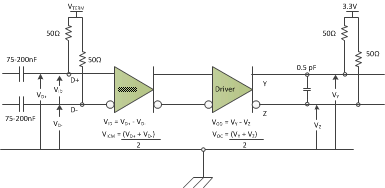 Figure 1. TMDS Main Link Test Circuit
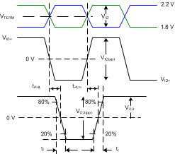 Figure 2. Input and Output Timing Measurements
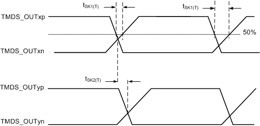 Figure 3. HDMI and DVI Sink TMDS Output Skew Measurements
 Figure 4. TMDS Main Link Common Mode Measurements
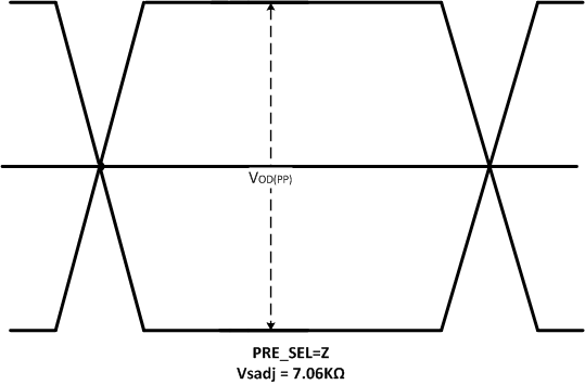 Figure 5. Output Differential Waveform 0 dB De-Emphasis
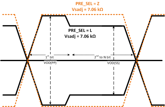 Figure 6. PRE_SEL = L for –2-dB De-Emphasis
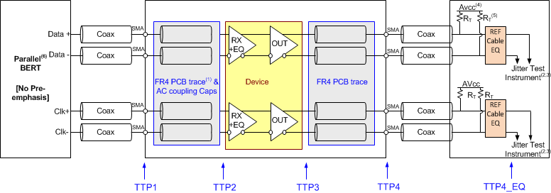
1. The FR4 trace between TTP1 and TTP2 is designed to emulate 1-8” of FR4, AC coupling cap, connector and another 1-2” of FR4. Trace width – 4 mils. 100-Ω differential impedance.
2. All jitter is measured at a BER of 10-9.
3. Residual jitter reflects the total jitter measured at TTP4 minus the jitter measured at TTP1.
4. AVCC = 3.3-V
5. RT = 50-Ω
6. The input signal from parallel bit error rate tester (BERT) does not have any pre-emphasis. Refer to Recommended Operating Conditions.
Figure 7. TMDS Output Jitter Measurement
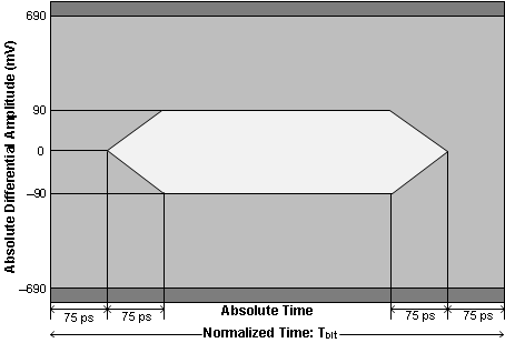
TMDS data eye mask at connector for clock frequency over 165 MHz.
Figure 8. Input Eye Mask at TTP2
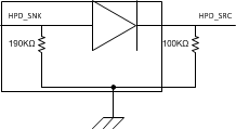 Figure 9. HPD Test Circuit
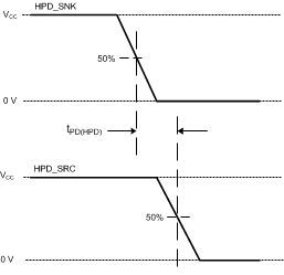 Figure 10. HPD Timing Diagram Number 1
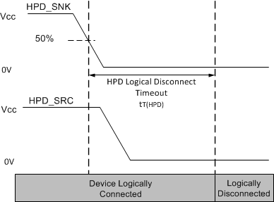 Figure 11. HPD Logic Disconnect Timeout
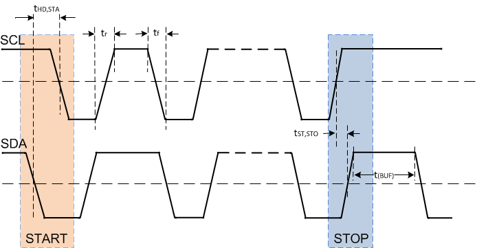 Figure 12. Start and Stop Condition Timing
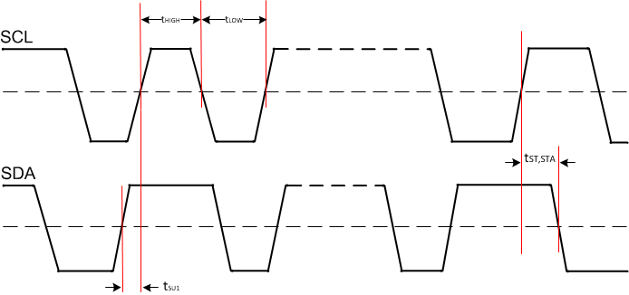 Figure 13. SCL and SDA Timing
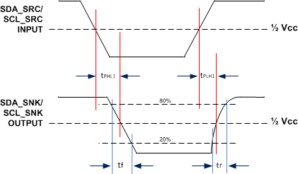 Figure 14. DDC Propagation Delay – Source to Sink
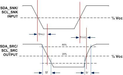 Figure 15. DDC Propagation Delay – Sink to Source
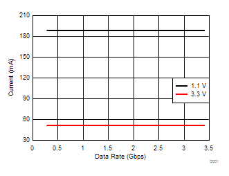
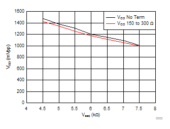
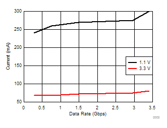
7.14 Typical Characteristics
