SLLSEV6C July 2017 – February 2021 TIOS101 , TIOS1013 , TIOS1015
PRODUCTION DATA
- 1 Features
- 2 Applications
- 3 Description
- 4 Revision History
- 5 Pin Configuration and Functions
- 6 Specifications
- 7 Parameter Measurement Information
-
8 Detailed Description
- 8.1 Overview
- 8.2 Functional Block Diagrams
- 8.3
Feature Description
- 8.3.1 Current Limit Configuration
- 8.3.2 Current Fault Detection, Indication and Auto Recovery
- 8.3.3 Thermal Warning, Thermal Shutdown
- 8.3.4 Fault Reporting (NFAULT)
- 8.3.5 Device Function Tables
- 8.3.6 The Integrated Voltage Regulator (LDO)
- 8.3.7 Reverse Polarity Protection
- 8.3.8 Integrated Surge Protection and Transient Waveform Tolerance
- 8.3.9 Power Up Sequence
- 8.3.10 Undervoltage Lock-Out (UVLO)
- 8.4 Device Functional Modes
- 9 Application Information Disclaimer
- 10Power Supply Recommendations
- 11Layout
- 12Device and Documentation Support
9.2.2.1 Maximum Junction Temperature Check
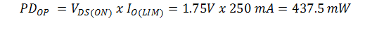
For a 200 mA current limit:
- The maximum driver output current limit, IO(LIM) = 250 mA (allowed for current limit tolerance).
- The maximum voltage drop across the high-side switch is given with VDS(ON) = 1.75 V.
This causes a power consumption of:
For a 5 mA LDO current output,

Total power dissipation,

Multiply this value with the Junction-to-ambient thermal resistance of θJA = 68.1°C/W (taken from the Section 6.4 table) to receive the difference between junction temperature, TJ, and ambient temperature, TA:

Add this value to the maximum ambient temperature of TA = 105°C to receive the final junction temperature:

As long as TJ-max is below the recommended maximum value of 150°C, no thermal shutdown will occur. However, thermal warning may occur as the junction temperature is greater than TWRN.
Note that the modeling of the complete system may be necessary to predict junction temperature in smaller PCBs and/or enclosures without air flow.