SLLU280A October 2017 – February 2022 TLIN1029-Q1 , TLIN2029-Q1
3 Board Layout
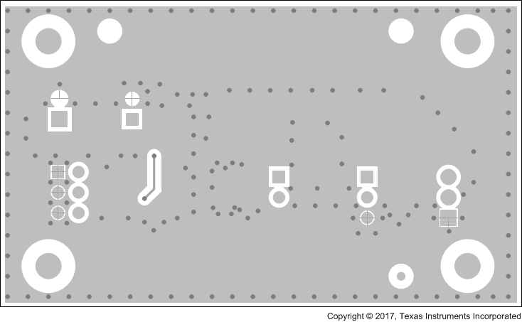
The board layout uses two layers (top and bottom) with most of the routing placed on the top layer (see Figure 3-1 and Figure 3-2). The TLIN2029A-Q1 device has a flow through pinout with the logic interface pins on one side of the device and the LIN bus pins on the other side resulting in simple and straight forward routing of signal and power nets.
Figure 3-1 Top Layer
 Figure 3-2 Bottom Layer