SLOA011B January 2018 – July 2021 LF347 , LF353 , LM348 , MC1458 , TL022 , TL061 , TL062 , TL071 , TL072 , UA741
- 1Introduction
- 2Non-Inverting Amplifier
- 3Inverting Amplifier
- 4Simplified Op Amp Circuit Diagram
-
5Op Amp Specifications
- 5.1 Absolute Maximum Ratings and Recommended Operating Condition
- 5.2 Input Offset Voltage
- 5.3 Input Current
- 5.4 Input Common Mode Voltage Range
- 5.5 Differential Input Voltage Range
- 5.6 Maximum Output Voltage Swing
- 5.7 Large Signal Differential Voltage Amplification
- 5.8 Input Parasitic Elements
- 5.9 Output Impedance
- 5.10 Common-Mode Rejection Ratio
- 5.11 Supply Voltage Rejection Ratio
- 5.12 Supply Current
- 5.13 Slew Rate at Unity Gain
- 5.14 Equivalent Input Noise
- 5.15 Total Harmonic Distortion Plus Noise
- 5.16 Unity-Gain Bandwidth and Phase Margin
- 5.17 Settling Time
- 6References
- 7Glossary
- 8Revision History
2 Non-Inverting Amplifier
An ideal op amp by itself is not a very useful device since any finite input signal would result in infinite output. By connecting external components around the ideal op amp, we can construct useful amplifier circuits. Figure 2-1 shows a basic op amp circuit, the non-inverting amplifier. The triangular gain block symbol is used to represent an ideal op amp. The input terminal marked with a + (Vp) is called the non-inverting input; – (Vn) marks the inverting input.
 Figure 2-1 Non-Inverting
Amplifier
Figure 2-1 Non-Inverting
AmplifierTo understand this circuit we must derive a relationship between the input voltage, Vi, and the output voltage, Vo.
Remembering that there is no loading at the input,
The voltage at Vn is derived from Vo via the resistor network, R1 and R2, so that,
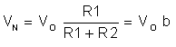
where,
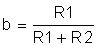
The parameter b is called the feedback factor because it represents the portion of the output that is fed back to the input.
Recalling the ideal model,
Substituting,
and collecting terms yield,
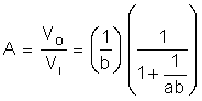
This result shows that the op amp circuit of Figure 2-1 is itself an amplifier with gain A. Since the polarity of Vi and VO are the same, it is referred to as a non-inverting amplifier.
A is called the close loop gain of the op amp circuit, whereas a is the open loop gain. The product ab is called the loop gain. This is the gain a signal would see starting at the inverting input and traveling in a clockwise loop through the op amp and the feedback network.