SLOA011B January 2018 – July 2021 LF347 , LF353 , LM348 , MC1458 , TL022 , TL061 , TL062 , TL071 , TL072 , UA741
- 1Introduction
- 2Non-Inverting Amplifier
- 3Inverting Amplifier
- 4Simplified Op Amp Circuit Diagram
-
5Op Amp Specifications
- 5.1 Absolute Maximum Ratings and Recommended Operating Condition
- 5.2 Input Offset Voltage
- 5.3 Input Current
- 5.4 Input Common Mode Voltage Range
- 5.5 Differential Input Voltage Range
- 5.6 Maximum Output Voltage Swing
- 5.7 Large Signal Differential Voltage Amplification
- 5.8 Input Parasitic Elements
- 5.9 Output Impedance
- 5.10 Common-Mode Rejection Ratio
- 5.11 Supply Voltage Rejection Ratio
- 5.12 Supply Current
- 5.13 Slew Rate at Unity Gain
- 5.14 Equivalent Input Noise
- 5.15 Total Harmonic Distortion Plus Noise
- 5.16 Unity-Gain Bandwidth and Phase Margin
- 5.17 Settling Time
- 6References
- 7Glossary
- 8Revision History
4 Simplified Op Amp Circuit Diagram
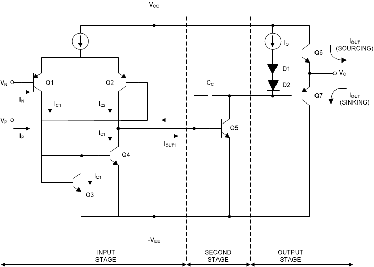
Real op amps are not ideal. They have limitations. To understand and discuss the origins of these limitations, see the simplified op amp circuit diagram shown in Figure 4-1.
 Figure 4-1 Simplified Op Amp Circuit
Diagram
Figure 4-1 Simplified Op Amp Circuit
DiagramAlthough simplified, this circuit contains the three basic elements normally found in op amps:
- Input stage
- Second stage
- Output stage
The function of the input stage is to amplify the input difference, Vp - Vn, and convert it to a single-ended signal. The second stage further amplifies the signal and provides frequency compensation. The output stage provides output drive capability.