SLOA011B January 2018 – July 2021 LF347 , LF353 , LM348 , MC1458 , TL022 , TL061 , TL062 , TL071 , TL072 , UA741
- 1Introduction
- 2Non-Inverting Amplifier
- 3Inverting Amplifier
- 4Simplified Op Amp Circuit Diagram
-
5Op Amp Specifications
- 5.1 Absolute Maximum Ratings and Recommended Operating Condition
- 5.2 Input Offset Voltage
- 5.3 Input Current
- 5.4 Input Common Mode Voltage Range
- 5.5 Differential Input Voltage Range
- 5.6 Maximum Output Voltage Swing
- 5.7 Large Signal Differential Voltage Amplification
- 5.8 Input Parasitic Elements
- 5.9 Output Impedance
- 5.10 Common-Mode Rejection Ratio
- 5.11 Supply Voltage Rejection Ratio
- 5.12 Supply Current
- 5.13 Slew Rate at Unity Gain
- 5.14 Equivalent Input Noise
- 5.15 Total Harmonic Distortion Plus Noise
- 5.16 Unity-Gain Bandwidth and Phase Margin
- 5.17 Settling Time
- 6References
- 7Glossary
- 8Revision History
5.5 Differential Input Voltage Range
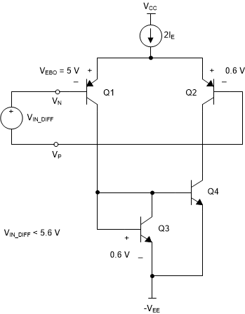
Differential input voltage range is normally specified in data sheets as an absolute maximum. Figure 5-4 illustrates this.
If the differential input voltage is greater than the base-emitter reverse break down voltage of input transistor Q1 plus the baseemitter forward breakdown voltage of Q2, then Q1’s BE junction will act like a zener diode. This is a destructive mode of operation and results in deterioration of Q1’s current gain. The same is true if VIN_DIFF is reversed, except Q2 breaks down.
 Figure 5-4 Differential-Mode Voltage Input Limit
Some devices have protection built into them, and the current into the input needs to be limited. Normally, differential input mode voltage limit is not a design issue.