SLUA748A December 2015 – April 2016 BQ25120 , BQ51003 , TPS61046 , TPS61240 , TPS62743
- Trademarks
- Power Management Reference Design for a Wearable Device with Wireless Charging Using the bq51003 and bq25120
- AExperimental Results
- Revision History
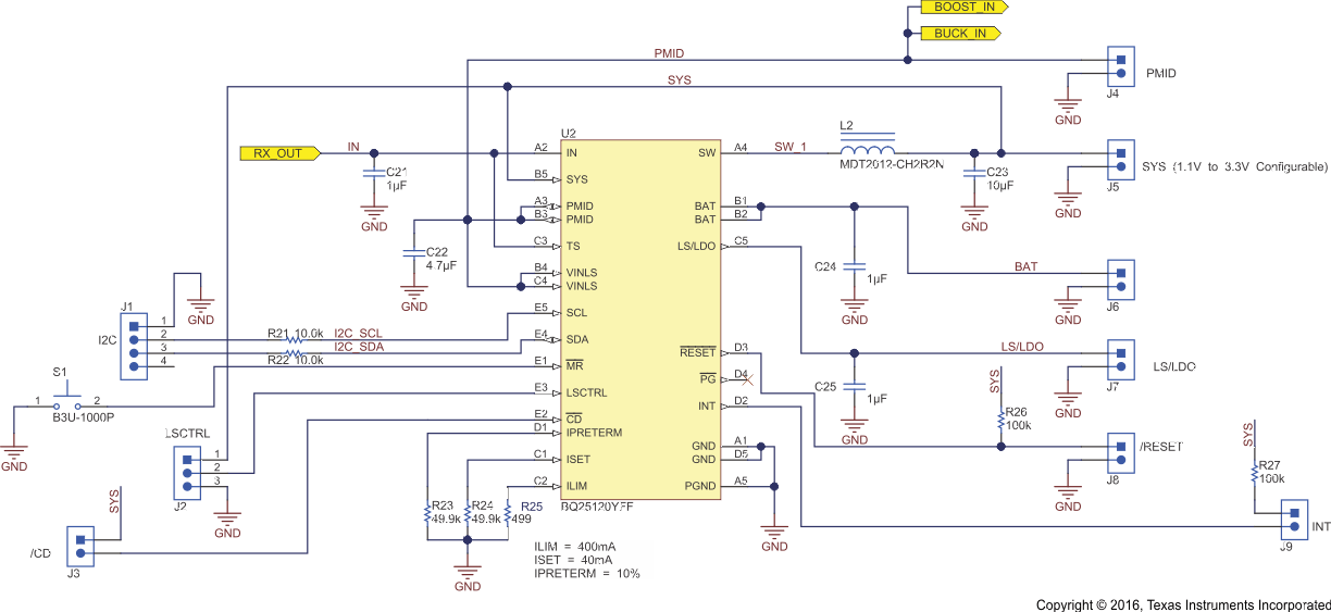
1.2 Battery Charger, MCU, Radio, and Sensor Power
The BQ25120 is a highly integrated battery charge management solution that integrates the most common functions for wearable devices: Linear charger, buck output, load switch or LDO, manual reset with timer, and battery voltage monitor. The integrated buck converter is a high efficiency, low Iq switcher using DCS control that extends light load efficiency down to 10 µA load currents. The low quiescent current during operation and shutdown enables maximum battery life. The BQ25120 has an I2C interface that allows configuration of key parameters including charge current, termination threshold, battery regulation voltage, DC/DC buck output voltage, load switch or LDO voltage, pushbutton timers and reset parameters, input current limit, battery undervoltage threshold, safety timer limit, battery monitor reads, and fault conditions. The design procedure for the BQ25120 can be found in the datasheet.
 Figure 4. Schematic of Battery Charger, MCU, Radio, and Sensor Power