SLUAAC4 October 2021 TPS92682-Q1
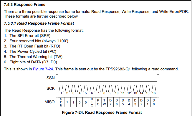
2 Response Frame
The command response frames are defined in the following portions of the TPS92682-Q1 Dual-Channel Constant-Voltage and Constant-Current Controller with SPI Data Sheet.
The following image illustrates the read response frame section of the data sheet.
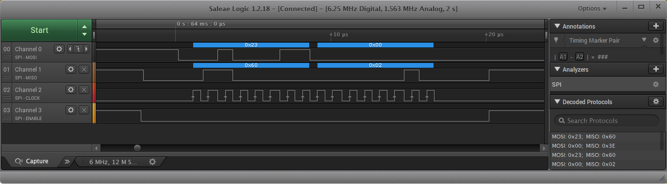
The command frame (Build a Frame) is SPI MOSI and the response is found in SPI MISO following it. The SPI MOSI command issued = 0x23 0x00. In this example the return (MISO result of 2 reads per SPI) has a status byte of 0x60 with a data byte of 0x02 indicating: CH2UV: Output undervoltage fault (CH2UV is disabled if 2PH is set to '1'). For a detailed explanation of the expected SPI bus return value with the TPS92682-Q1, visit the TI E2E™ support forum.
The following image shows the Read Fault Register 0x11 (FLT1).
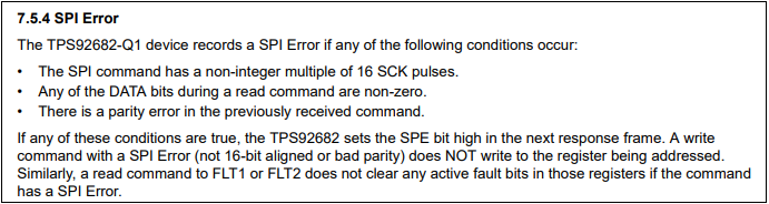
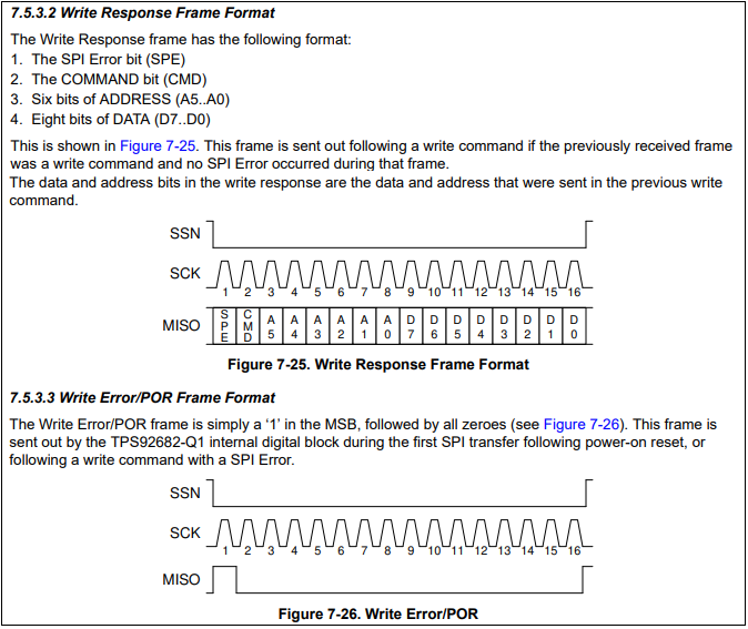
The following image shows the write response frame format, write error/POR frame format SPI error sections from the data sheet:
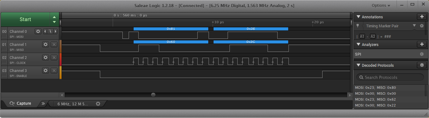
The following command frame is SPI MOSI and the response is found in SPI MISO after it. The SPI MOSI command issued = 0x81 0x3E. In this example, the return (MISO result of previous read of register 0x00) has a status byte of 0x60 with a data byte of 0x3c indicating: default power up value for register 0x00. For a detailed explanation of the expected SPI bus return value with the TPS92682-Q1, visit the TI E2E™ support forum.
The following image shows the Write Enable Register 0x00 (EN).