SLUAAJ5 April 2022 TPS565242 , TPS565247 , TPS566242 , TPS566247
2 Improve Thermal Performance from IC Independently
First, from TPS566242/7 independently, it optimizes pin-out definition. Figure 2-1 shows pin-out. The device integrates BST pin and add one AGND for PIN4. This pin-out makes layout very easy on board. Figure 2-1 shows suggested layout. In top layer, it places nearly all line, especially power line as Figure 2-2. It is recommended to connect GND and AGND together to increase GND area to improve thermal performance. FB line goes through on bottom layer to avoid to be affected by switching noise Figure 2-3.
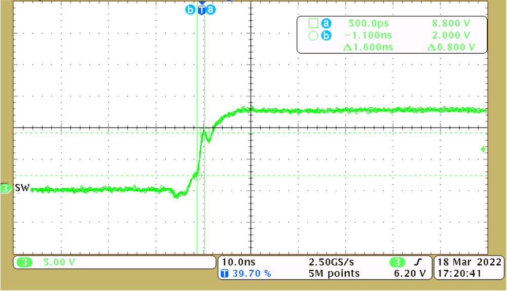
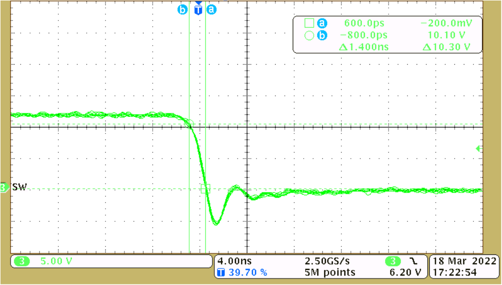
TPS566242/7 integrates small Rdson of 27.7 mohm for high side and 14.8 mohm low side. Small Rdson will cause small conducting loss which will be helpful for high efficiency. And it also increases driving slew rate to reduce switching loss. Below Figure 2-4 and Figure 2-5 show the TPS566242 SW waveform at 12-V Vin to 5-V Vout at 6-A loading. For the rising edge, the slew rate could get 4.25-V/ns. At the same time, this part uses special driver design to decrease switching ring voltage. For the falling edge, the slew rate could get 7.35-V/ns. This fast switching slew rate decreases switching loss which is also helpful for high efficiency.
 Figure 2-4 TPS566242 Rising
Edge
 Figure 2-5 TPS566242 Falling
Edge