SLUS720F February 2007 – June 2019 TPS40195
PRODUCTION DATA.
- 1 Features
- 2 Applications
- 3 Description
- 4 Revision History
- 5 Description (continued)
- 6 Pin Configuration and Functions
- 7 Specifications
- 8 Detailed Description
-
9 Application and Implementation
- 9.1 Application Information
- 9.2
Typical Applications
- 9.2.1
Typical Application 1
- 9.2.1.1 Design Requirements
- 9.2.1.2
Detailed Design Procedure
- 9.2.1.2.1 Output Inductor, LOUT
- 9.2.1.2.2 Output Capacitor, COUT
- 9.2.1.2.3 Input Capacitor, CIN
- 9.2.1.2.4 Switching MOSFET, QSW
- 9.2.1.2.5 Rectifier MOSFET, QSR
- 9.2.1.2.6
Component Selection for the TPS40195
- 9.2.1.2.6.1 Timing Resistor, RT
- 9.2.1.2.6.2 Setting UVLO
- 9.2.1.2.6.3 Setting the Soft-Start Time
- 9.2.1.2.6.4 Short-Circuit Protection, RILIM
- 9.2.1.2.6.5 Voltage Decoupling Capacitors, CBP, and CVDD
- 9.2.1.2.6.6 Boost Voltage, CBOOST and DBOOST (optional)
- 9.2.1.2.6.7 Closing the Feedback Loop RZ1, RP1, RPZ2, RSET1, RSET2, CZ2, CP2 AND CPZ1
- 9.2.1.2.7 Application Curve
- 9.2.2 Typical Application 2
- 9.2.3 Typical Application 3
- 9.2.1
Typical Application 1
- 10Layout
- 11Device and Documentation Support
- 12Mechanical, Packaging, and Orderable Information
9.2.1.2.6.7 Closing the Feedback Loop RZ1, RP1, RPZ2, RSET1, RSET2, CZ2, CP2 AND CPZ1
A graphical method is used to select the compensation components. This is a standard feedforward buck converter. Its PWM gain is given by the following equation.

The gain of the output LC filter is given in Equation 38.

The equation for the PWM and LC gain is:

To plot this on a Bode plot the DC gain must be expressed in dB. The DC gain is equal to KPWM. To express this in dB we take its LOG and multiple by 20. For this converter the DC gain is:

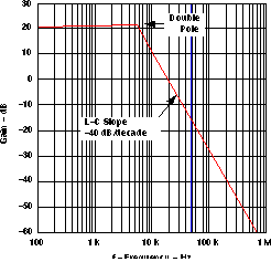
Also calculate the pole and zero frequencies. A double pole is associated with the LC and a zero is associated with the ESR of the output capacitance. The frequency at where these occur can be calculated using Equation 41.


A Bode plot of the PWM and LC filter is shown in Figure 23.
 Figure 23. PWM and L-C Filter Gain
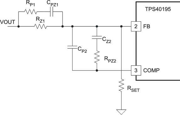
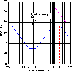
 A Type-III compensation network, shown in Figure 24, is used for this design. A typical bode plot of a Type-III compensation network is shown below in Figure 25.
 Figure 24. Type III Compensation Schematic
  Figure 25. Type-III Compensation Network Typical Bode Plot
 The output voltage, the high-frequency gain and the break (pole and zero) frequencies are calculated using the following equations.


Steps in closing the feedback loop.
- Place one zero well below the L-C double pole at 5.8 kHz (fZ1=2.1 kHz)
- Place the second zero near the double pole fZ2 at 5.8 kHz.
- Place one pole well above the desired cross over frequency, selected as one sixth the switching frequency, fCO1 = 50 kHz, fP1 = 300 kHz
- Place the second pole near the ESR zero of the output capacitors of 318 kHz. fP2 = 318 kHz
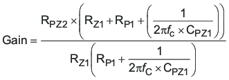
- The high frequency gain must be such that the over all system has 0 dB at the required crossover frequency. This gain is -1 times the sum of the modulator gain and the gain of the output stage at the crossover frequency of 50 kHz.
Using these values and the above equations calculate the setpoint and the Rs and Cs around the compensation network using the following procedure.
- Set RZ1 = 51 kΩ
- Calculate RSET using Equation 43. For this module RSET = a standard 1% value = 24.9 kΩ.
- Using Equation 48 and fZ1 = 1.8 kHz, CPZ1 can be calculated to be 1500 pF, FP1 and Equation 46 yields RP1 to be 363 Ω and the standard value 357 Ω is used.
- From Figure 23, the required gain is calculated at 15.8 dB. Equation 45 sets the value for RPZ2. A resistor for RPZ2 with value of 12.7 kΩ is used. CZ2 is calculated using Equation 49 and the desired frequency for the second zero, CZ2 = 1475 pF. A 2200 pF capacitor is used.
- CP2 is calculated using the second pole frequency and Equation 47, CP2 = 37 pF. A 33-pf capacitor is used.