SLUSAH1E MAY   2011  – July 2018 TPS51206

PRODUCTION DATA.  

  1. Features
  2. Applications
  3. Description
    1.     Device Images
      1.      Simplified Application
  4. Revision History
  5. Pin Configuration and Functions
    1.     Pin Functions
  6. Specifications
    1. 6.1 Absolute Maximum Ratings
    2. 6.2 ESD Ratings
    3. 6.3 Recommended Operating Conditions
    4. 6.4 Thermal Information
    5. 6.5 Electrical Characteristics
    6. 6.6 Typical Characteristics
  7. Detailed Description
    1. 7.1 Overview
    2. 7.2 Functional Block Diagram
    3. 7.3 Feature Description
      1. 7.3.1 VTT Sink and Source Regulator
      2. 7.3.2 VTTREF
      3. 7.3.3 VDD Undervoltage Lockout Protection
      4. 7.3.4 VTT Current Limit
      5. 7.3.5 Overtemperature Protection
      6. 7.3.6 Power On and Off Sequence
    4. 7.4 Device Functional Modes
      1. 7.4.1 Power State Control
  8. Application and Implementation
    1. 8.1 Application Information
    2. 8.2 Typical Applications
      1. 8.2.1 VLDOIN = VDDQ Configuration
        1. 8.2.1.1 Design Requirements
        2. 8.2.1.2 Detailed Design Procedure
          1. 8.2.1.2.1 VDD Capacitor
          2. 8.2.1.2.2 VLDOIN Capacitor
          3. 8.2.1.2.3 VTTREF Capacitor
          4. 8.2.1.2.4 VTT Capacitor
          5. 8.2.1.2.5 VTTSNS Connection
          6. 8.2.1.2.6 VDDQSNS Connection
        3. 8.2.1.3 Application Curves
      2. 8.2.2 VLDOIN Separated from VDDQ Configuration
        1. 8.2.2.1 Design Requirements
        2. 8.2.2.2 Detailed Design Procedure
        3. 8.2.2.3 Application Curves
  9. Power Supply Recommendations
  10. 10Layout
    1. 10.1 Layout Guidelines
    2. 10.2 Layout Example
    3. 10.3 Thermal Considerations
  11. 11Device and Documentation Support
    1. 11.1 Device Support
      1. 11.1.1 Third-Party Products Disclaimer
    2. 11.2 Receiving Notification of Documentation Updates
    3. 11.3 Community Resources
    4. 11.4 Trademarks
    5. 11.5 Electrostatic Discharge Caution
    6. 11.6 Glossary
  12. 12Mechanical, Packaging, and Orderable Information

VTTSNS Connection

To achieve tight regulation with minimum effect of trace resistance, a remote sensing terminal, the VTTSNS pin should be connected to the positive terminal of the VTT pin output capacitor(s) as a separate trace from the high-current path from VTT. Consider adding a low-pass R-C filter at the VTTSNS pin in case the ESR of the VTT output capacitor(s) is larger than 2 mΩ. The R-C filter time constant should be approximately the same or slightly lower than the time constant of the VTT output capacitance and ESR.
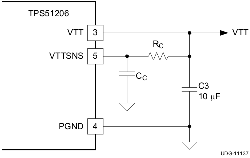
TPS51206 v11037_lusah1.gifFigure 25. R-C Filter for VTTSNS