SLUSCO1A June 2017 – April 2018 UCC27212
PRODUCTION DATA.
6.6 Switching Characteristics
over operating free-air temperature range (unless otherwise noted)| PARAMETER | TEST CONDITIONS | MIN | TYP | MAX | UNIT | |
|---|---|---|---|---|---|---|
| PROPAGATION DELAYS, VDD = VHB = 12 V | ||||||
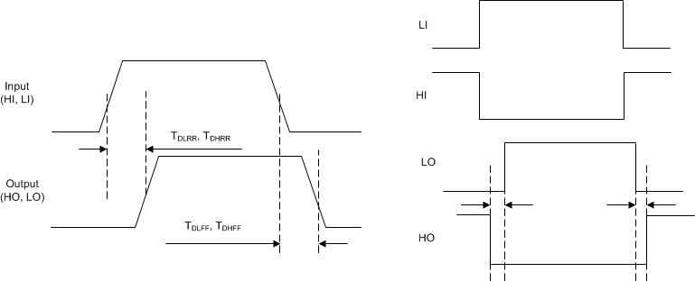
| TDLFF | VLI falling to VLO falling | CLOAD = 0 | 10 | 16 | 30 | ns |
| TDHFF | VHI falling to VHO falling | CLOAD = 0 | 10 | 16 | 30 | ns |
| TDLRR | VLI rising to VLO rising | CLOAD = 0 | 10 | 20 | 42 | ns |
| TDHRR | VHI rising to VHO rising | CLOAD = 0 | 10 | 20 | 42 | ns |
| PROPAGATION DELAYS, VDD = VHB = 6.8 V | ||||||
| TDLFF | VLI falling to VLO falling | CLOAD = 0 | 10 | 24 | 50 | ns |
| TDHFF | VHI falling to VHO falling | CLOAD = 0 | 10 | 24 | 50 | ns |
| TDLRR | VLI rising to VLO rising | CLOAD = 0 | 13 | 28 | 57 | ns |
| TDHRR | VHI rising to VHO rising | CLOAD = 0 | 13 | 28 | 57 | ns |
| DELAY MATCHING, VDD = VHB = 12 V | ||||||
| TMON | From HO OFF to LO ON | TJ = 25°C | 4 | 9.5 | ns | |
| TJ = –40°C to +140°C | 4 | 17 | ns | |||
| TMOFF | From LO OFF to HO ON | TJ = 25°C | 4 | 9.5 | ns | |
| TJ = –40°C to +140°C | 4 | 17 | ns | |||
| DELAY MATCHING, VDD = VHB = 6.8 V | ||||||
| TMON | From HO OFF to LO ON | TJ = 25°C | 8 | ns | ||
| TJ = –40°C to +140°C | 8 | 18 | ns | |||
| TMOFF | From LO OFF to HO ON | TJ = 25°C | 6 | ns | ||
| TJ = –40°C to +140°C | 6 | 18 | ns | |||
| OUTPUT RISE AND FALL TIME, VDD = VHB = 12 V | ||||||
| tR | LO rise time | CLOAD = 1000 pF, from 10% to 90% | 7.8 | ns | ||
| tR | HO rise time | CLOAD = 1000 pF, from 10% to 90% | 7.8 | ns | ||
| tF | LO fall time | CLOAD = 1000 pF, from 90% to 10% | 6.0 | ns | ||
| tF | HO fall time | CLOAD = 1000 pF, from 90% to 10% | 6.0 | ns | ||
| tR | LO, HO | CLOAD = 0.1 µF, (3 V to 9 V) | 0.36 | 0.6 | µs | |
| tF | LO, HO | CLOAD = 0.1 µF, (9 V to 3 V) | 0.20 | 0.4 | µs | |
| OUTPUT RISE AND FALL TIME, VDD = VHB = 6.8 V | ||||||
| tR | LO rise time | CLOAD = 1000 pF, from 10% to 90% | 9.5 | ns | ||
| tR | HO rise time | CLOAD = 1000 pF, from 10% to 90% | 13.0 | ns | ||
| tF | LO fall time | CLOAD = 1000 pF, from 90% to 10% | 9.5 | ns | ||
| tF | HO fall time | CLOAD = 1000 pF, from 90% to 10% | 13.0 | ns | ||
| tR | LO, HO | CLOAD = 0.1 µF, (30% to 70%) | 0.45 | 0.7 | µs | |
| tF | LO, HO | CLOAD = 0.1 µF, (70% to 30%) | 0.2 | 0.5 | µs | |
| MISCELLANEOUS | ||||||
| Minimum input pulse width that changes the output | 100 | ns | ||||
| Bootstrap diode turnoff time (1)(2) | IF = 20 mA, IREV = 0.5 A (3) | 20 | ns | |||
| Extended output pulse | when VDD = VHB = 6.8 V, VHS = 100 V, and input pulse width is 100 ns | 325 | ns | |||
(1) Ensured by design.
(2) IF: Forward current applied to bootstrap diode, IREV: Reverse current applied to bootstrap diode.
(3) Typical values for TA = 25°C.
 Figure 1. Timing Diagram