SLUSCO1A June   2017  – April 2018 UCC27212

PRODUCTION DATA.  

  1. Features
  2. Applications
  3. Description
    1.     Device Images
      1.      Typical Application Diagram
      2.      Propagation Delays vs Supply Voltage T = 25°C
  4. Revision History
  5. Pin Configuration and Functions
    1.     Pin Functions
  6. Specifications
    1. 6.1 Absolute Maximum Ratings
    2. 6.2 ESD Ratings
    3. 6.3 Recommended Operating Conditions
    4. 6.4 Thermal Information
    5. 6.5 Electrical Characteristics
    6. 6.6 Switching Characteristics
    7. 6.7 Typical Characteristics
  7. Detailed Description
    1. 7.1 Overview
    2. 7.2 Functional Block Diagram
    3. 7.3 Feature Description
      1. 7.3.1 Input Stages
      2. 7.3.2 Undervoltage Lockout (UVLO)
      3. 7.3.3 Level Shift
      4. 7.3.4 Boot Diode
      5. 7.3.5 Output Stages
    4. 7.4 Device Functional Modes
  8. Application and Implementation
    1. 8.1 Application Information
    2. 8.2 Typical Application
      1. 8.2.1 Design Requirements
      2. 8.2.2 Detailed Design Procedure
        1. 8.2.2.1 Power Dissipation
      3. 8.2.3 Application Curves
  9. Power Supply Recommendations
  10. 10Layout
    1. 10.1 Layout Guidelines
    2. 10.2 Layout Example
      1. 10.2.1 Thermal Considerations
  11. 11Device and Documentation Support
    1. 11.1 Documentation Support
      1. 11.1.1 Related Documentation
    2. 11.2 Receiving Notification of Documentation Updates
    3. 11.3 Community Resources
    4. 11.4 Trademarks
    5. 11.5 Electrostatic Discharge Caution
    6. 11.6 Glossary
  12. 12Mechanical, Packaging, and Orderable Information

Typical Characteristics

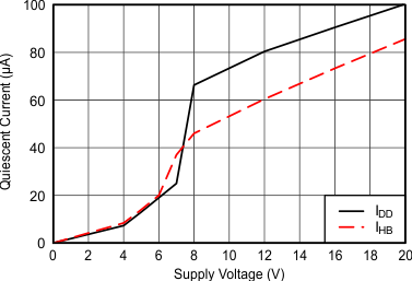
UCC27212 0001_IDD_IHB_vs_VDD_VHB_lusat7.gif
T = 25°C
Figure 2. Quiescent Current vs Supply Voltage
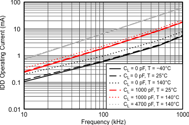
UCC27212 0003_UCC27211_IDDO_vs_Freq_lusat7.gif
VDD = 12 V
Figure 4. IDD Operating Current vs Frequency
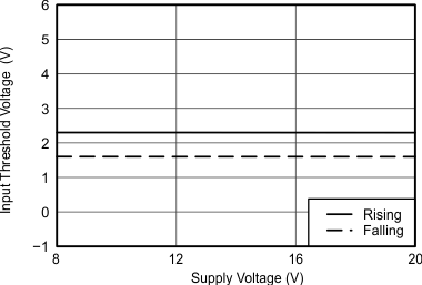
UCC27212 0005_VIHL_vs_VDD_lusat7.gif
T = 25°C
Figure 6. Input Threshold vs Supply Voltage
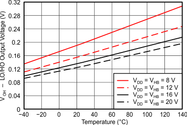
UCC27212 0007_VOH_vs_Temp_lusat7.gif
IHO = ILO = 100 mA
Figure 8. LO and HO High-Level Output Voltage
vs Temperature
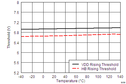
UCC27212 0009_UVLO_vs_Temp_lusat7.png
Figure 10. Undervoltage Lockout Threshold
vs Temperature
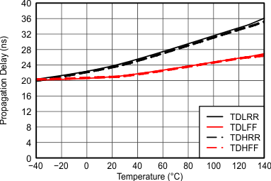
UCC27212 0011_UCC27210_Delay_vs_Temp_lusat7.gif
VDD = VHB = 12 V
Figure 12. Propagation Delays vs Temperature
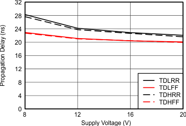
UCC27212 0013_UCC27210_Delay_vs_VDD_lusat7.gif
T = 25°C
Figure 14. Propagation Delays vs Supply Voltage
(VDD = VHB)
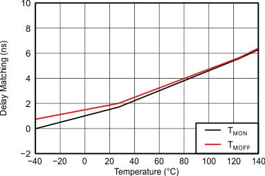
UCC27212 0015_DelayMatching_vs_Temp_lusat7.gif
VDD = VHB = 12 V
Figure 16. Delay Matching vs Temperature
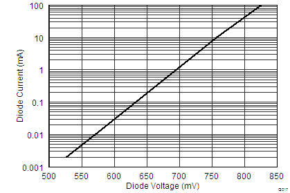
UCC27212 0017_DiodeCurrent_vs_DiodeVoltage_lusat7.png
Figure 18. Diode Current vs Diode Voltage
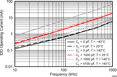
UCC27212 0002_UCC27210_IDDO_vs_Freq_lusat7.gif
VDD = 12 V
Figure 3. IDD Operating Current vs Frequency
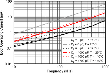
UCC27212 0004_IHBO_vs_Freq_lusat7.gif
VHB – VHS = 12 V
Figure 5. Boot Voltage Operating Current vs
Frequency (HB To HS)
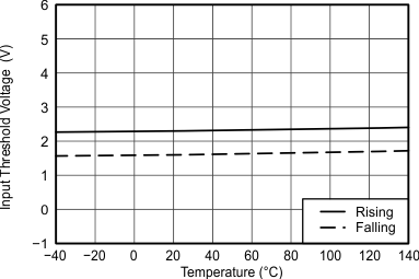
UCC27212 0006_VIHL_vs_Temp_lusat7.gif
VDD = 12 V
Figure 7. Input Thresholds vs Temperature
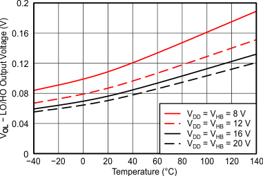
UCC27212 0008_VOL_vs_Temp_lusat7.gif
IHO = ILO = 100 mA
Figure 9. LO and HO Low-Level Output Voltage
vs Temperature
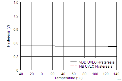
UCC27212 0010_UVLO_HYS_vs_Temp_lusat7.png
Figure 11. Undervoltage Lockout Threshold Hysteresis
vs Temperature
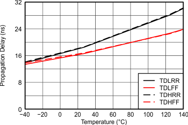
UCC27212 0012_UCC27211_Delay_vs_Temp_lusat7.gif
VDD = VHB = 12 V
Figure 13. Propagation Delays vs Temperature
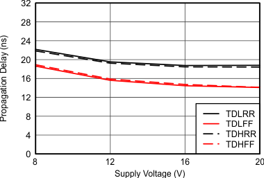
UCC27212 0014_UCC27211_Delay_vs_VDD_lusat7.gif
T = 25°C
Figure 15. Propagation Delays vs Supply Voltage
(VDD = VHB)
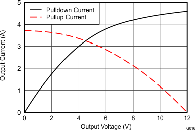
UCC27212 out_new_sluscg0.gif
VDD = VHB = 12 V
Figure 17. Output Current vs Output Voltage