SLUSDC0C October   2018  – November 2021 UCC21530

PRODUCTION DATA  

  1. Features
  2. Applications
  3. Description
  4. Revision History
  5. Pin Configuration and Functions
  6. Specifications
    1. 6.1  Absolute Maximum Ratings
    2. 6.2  ESD Ratings
    3. 6.3  Recommended Operating Conditions
    4. 6.4  Thermal Information
    5. 6.5  Power Ratings
    6. 6.6  Insulation Specifications
    7. 6.7  Safety-Related Certifications
    8. 6.8  Safety-Limiting Values
    9. 6.9  Electrical Characteristics
    10. 6.10 Switching Characteristics
    11. 6.11 Insulation Characteristics Curves
    12. 6.12 Typical Characteristics
  7. Parameter Measurement Information
    1. 7.1 Propagation Delay and Pulse Width Distortion
    2. 7.2 Rising and Falling Time
    3. 7.3 Input and Enable Response Time
    4. 7.4 Programable Dead Time
    5. 7.5 Power-Up UVLO Delay to OUTPUT
    6. 7.6 CMTI Testing
  8. Detailed Description
    1. 8.1 Overview
    2. 8.2 Functional Block Diagram
    3. 8.3 Feature Description
      1. 8.3.1 VDD, VCCI, and Under Voltage Lock Out (UVLO)
      2. 8.3.2 Input and Output Logic Table
      3. 8.3.3 Input Stage
      4. 8.3.4 Output Stage
      5. 8.3.5 Diode Structure in UCC21530
    4. 8.4 Device Functional Modes
      1. 8.4.1 Enable Pin
      2. 8.4.2 Programmable Dead Time (DT) Pin
        1. 8.4.2.1 DT Pin Tied to VCC
        2. 8.4.2.2 DT Pin Connected to a Programming Resistor between DT and GND Pins
  9. Application and Implementation
    1. 9.1 Application Information
    2. 9.2 Typical Application
      1. 9.2.1 Design Requirements
      2. 9.2.2 Detailed Design Procedure
        1. 9.2.2.1 Designing INA/INB Input Filter
        2. 9.2.2.2 Select Dead Time Resistor and Capacitor
        3. 9.2.2.3 Gate Driver Output Resistor
        4. 9.2.2.4 Estimate Gate Driver Power Loss
        5. 9.2.2.5 Estimating Junction Temperature
        6. 9.2.2.6 Selecting VCCI, VDDA/B Capacitor
          1. 9.2.2.6.1 Selecting a VCCI Capacitor
        7. 9.2.2.7 Other Application Example Circuits
      3. 9.2.3 Application Curves
  10. 10Power Supply Recommendations
  11. 11Layout
    1. 11.1 Layout Guidelines
      1. 11.1.1 Component Placement Considerations
      2. 11.1.2 Grounding Considerations
      3. 11.1.3 High-Voltage Considerations
      4. 11.1.4 Thermal Considerations
    2. 11.2 Layout Example
  12. 12Device and Documentation Support
    1. 12.1 Documentation Support
      1. 12.1.1 Related Documentation
    2. 12.2 Receiving Notification of Documentation Updates
    3. 12.3 Support Resources
    4. 12.4 Trademarks
    5. 12.5 Electrostatic Discharge Caution
    6. 12.6 Glossary

Insulation Characteristics Curves

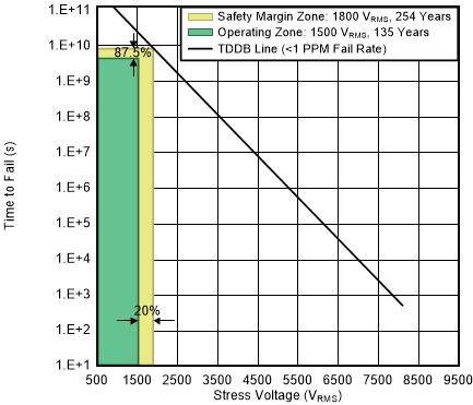
GUID-967444FC-0B48-4E07-9714-51545E19D935-low.gifFigure 6-1 Reinforced Isolation Capacitor Life Time Projection
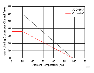
GUID-3FF5E7FF-9147-4C9B-BD20-7BE88BD01679-low.gifFigure 6-2 Thermal Derating Curve for Safety-Related Limiting Current (Current in Each Channel with Both Channels Running Simultaneously)
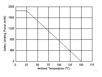
GUID-B35DFD17-CBA3-4576-937E-E48D03DE98AB-low.gifFigure 6-3 Thermal Derating Curve for Safety-Related Limiting Power