SLUSDC0C October 2018 – November 2021 UCC21530
PRODUCTION DATA
- 1 Features
- 2 Applications
- 3 Description
- 4 Revision History
- 5 Pin Configuration and Functions
-
6 Specifications
- 6.1 Absolute Maximum Ratings
- 6.2 ESD Ratings
- 6.3 Recommended Operating Conditions
- 6.4 Thermal Information
- 6.5 Power Ratings
- 6.6 Insulation Specifications
- 6.7 Safety-Related Certifications
- 6.8 Safety-Limiting Values
- 6.9 Electrical Characteristics
- 6.10 Switching Characteristics
- 6.11 Insulation Characteristics Curves
- 6.12 Typical Characteristics
- 7 Parameter Measurement Information
- 8 Detailed Description
-
9 Application and Implementation
- 9.1 Application Information
- 9.2
Typical Application
- 9.2.1 Design Requirements
- 9.2.2 Detailed Design Procedure
- 9.2.3 Application Curves
- 10Power Supply Recommendations
- 11Layout
- 12Device and Documentation Support
8.4.2.2 DT Pin Connected to a Programming Resistor between DT and GND Pins
Program tDT by placing a resistor, RDT, between the DT pin and GND. TI recommends bypassing this pin with a ceramic capacitor, 2.2 nF or greater, close to DT pin to achieve better noise immunity. The appropriate RDT value can be determined from:
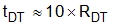
where
- tDT is the programmed dead time, in nanoseconds.
- RDT is the value of resistance between DT pin and GND, in kilo-ohms.
The steady state voltage at the DT pin is about 0.8 V. RDT programs a small current at this pin, which sets the dead time. As the value of RDT increases, the current sourced by the DT pin decreases. The DT pin current will be less than 10 µA when RDT = 100 kΩ. For larger values of RDT, TI recommends placing RDT and a ceramic capacitor, 2.2 nF or greater, as close to the DT pin as possible to achieve greater noise immunity and better dead time matching between both channels.
The falling edge of an input signal initiates the programmed dead time for the other signal. The programmed dead time is the minimum enforced duration in which both outputs are held low by the driver. The outputs may also be held low for a duration greater than the programmed dead time, if the INA and INB signals include a dead time duration greater than the programmed minimum. If both inputs are high simultaneously, both outputs will immediately be set low. This feature is used to prevent shoot-through in half-bridge applications, and it does not affect the programmed dead time setting for normal operation. Various driver dead time logic operating conditions are illustrated and explained in .
 Figure 8-4 Input and
Output Logic Relationship With Input Signals
Figure 8-4 Input and
Output Logic Relationship With Input SignalsCondition A: INB goes low, INA goes high. INB sets OUTB low immediately and assigns the programmed dead time to OUTA. OUTA is allowed to go high after the programmed dead time.
Condition B: INB goes high, INA goes low. Now INA sets OUTA low immediately and assigns the programmed dead time to OUTB. OUTB is allowed to go high after the programmed dead time.
Condition C: INB goes low, INA is still low. INB sets OUTB low immediately and assigns the programmed dead time for OUTA. In this case, the input signal’s own dead time is longer than the programmed dead time. Thus, when INA goes high, it immediately sets OUTA high.
Condition D: INA goes low, INB is still low. INA sets OUTA low immediately and assigns the programmed dead time to OUTB. INB’s own dead time is longer than the programmed dead time. Thus, when INB goes high, it immediately sets OUTB high.
Condition E: INA goes high, while INB and OUTB are still high. To avoid overshoot, INA immediately pulls OUTB low and keeps OUTA low. After some time OUTB goes low and assigns the programmed dead time to OUTA. OUTB is already low. After the programmed dead time, OUTA is allowed to go high.
Condition F: INB goes high, while INA and OUTA are still high. To avoid overshoot, INB immediately pulls OUTA low and keeps OUTB low. After some time OUTA goes low and assigns the programmed dead time to OUTB. OUTA is already low. After the programmed dead time, OUTB is allowed to go high.