SLUSDC0C October 2018 – November 2021 UCC21530
PRODUCTION DATA
- 1 Features
- 2 Applications
- 3 Description
- 4 Revision History
- 5 Pin Configuration and Functions
-
6 Specifications
- 6.1 Absolute Maximum Ratings
- 6.2 ESD Ratings
- 6.3 Recommended Operating Conditions
- 6.4 Thermal Information
- 6.5 Power Ratings
- 6.6 Insulation Specifications
- 6.7 Safety-Related Certifications
- 6.8 Safety-Limiting Values
- 6.9 Electrical Characteristics
- 6.10 Switching Characteristics
- 6.11 Insulation Characteristics Curves
- 6.12 Typical Characteristics
- 7 Parameter Measurement Information
- 8 Detailed Description
-
9 Application and Implementation
- 9.1 Application Information
- 9.2
Typical Application
- 9.2.1 Design Requirements
- 9.2.2 Detailed Design Procedure
- 9.2.3 Application Curves
- 10Power Supply Recommendations
- 11Layout
- 12Device and Documentation Support
3 Description
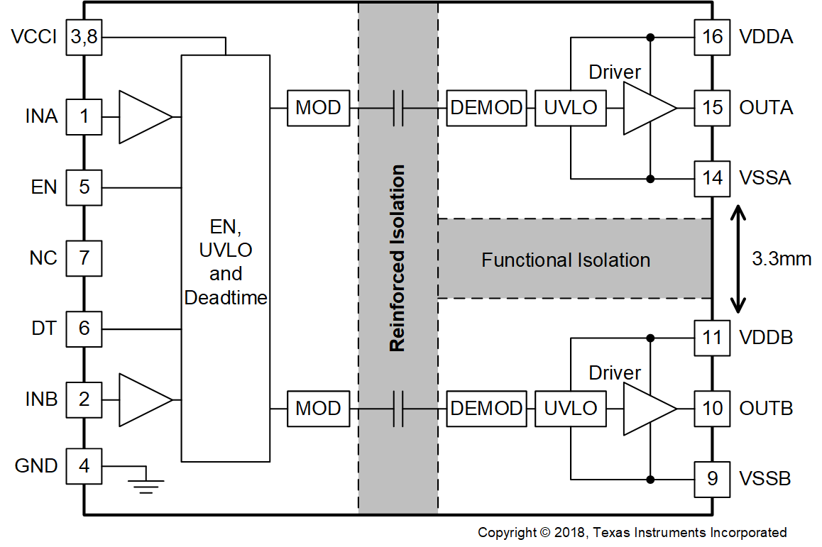
The UCC21530 is an isolated dual-channel gate driver with 4-A source and 6-A sink peak current. It is designed to drive IGBTs, Si MOSFETs, and SiC MOSFETs up to 5-MHz with best-in-class propagation delay and pulse-width distortion.
The input side is isolated from the two output drivers by a 5.7-kVRMS reinforced isolation barrier, with a minimum of 100-V/ns common-mode transient immunity (CMTI). Internal functional isolation between the two secondary-side drivers allows a working voltage of up to 1850 V.
This device can be configured as two low-side drivers, two high-side drivers, or a half-bridge driver with programmable dead time (DT). The EN pin pulled low shuts down both outputs simultaneously and allows for normal operation when left open or pulled high. As a fail-safe measure, primary-side logic failures force both outputs low.
The device accepts VDD supply voltages up to 25 V. A wide input VCCI range from 3 V to 18 V makes the driver suitable for interfacing with both analog and digital controllers. All the supply voltage pins have under voltage lock-out (UVLO) protection.
| PART NUMBER | PACKAGE | BODY SIZE (NOM) |
|---|---|---|
| UCC21530 | DWK SOIC (14) | 10.30 mm × 7.50 mm |
 Functional Block Diagram