SLUUCN1C June 2022 – December 2022 UCC28C50 , UCC28C50-Q1 , UCC28C51 , UCC28C51-Q1 , UCC28C52 , UCC28C52-Q1 , UCC28C53 , UCC28C53-Q1 , UCC28C54 , UCC28C54-Q1 , UCC28C55 , UCC28C55-Q1 , UCC28C56H , UCC28C56H-Q1 , UCC28C56L , UCC28C56L-Q1 , UCC28C57H , UCC28C57H-Q1 , UCC28C57L , UCC28C57L-Q1 , UCC28C58 , UCC28C58-Q1 , UCC28C59 , UCC28C59-Q1
- Trademarks
- 1General Texas Instruments High Voltage Evaluation (TI HV EVM) User Safety Guidelines
- 2Description
- 3Schematic Diagram
- 4EVM Setup and Operation
-
5Performance Data
- 5.1 Efficiency Versus Load, 10% to 100% Load
- 5.2 Efficiency Versus VIN at 100% Load
- 5.3 Power Loss Versus Load, 10% to 100% Load
- 5.4 Load Regulation, 10% to 100% Load
- 5.5 Light Load Regulation, 0-mA to 200-mA Load
- 5.6 Line Regulation, Various Loads
- 5.7 Startup Waveforms
- 5.8 Shutdown Waveforms
- 5.9 Output Voltage Ripple
- 5.10 Steady State Switching Waveforms
- 5.11 Transient Load Waveforms
- 5.12 Over Current and Short Circuit Protections
- 5.13 Stability Measurements
- 5.14 Thermal Measurements
- 6Assembly and Printed Circuit Board (PCB)
- 7Bill of Materials (BOM)
- 8Revision History
2 Description
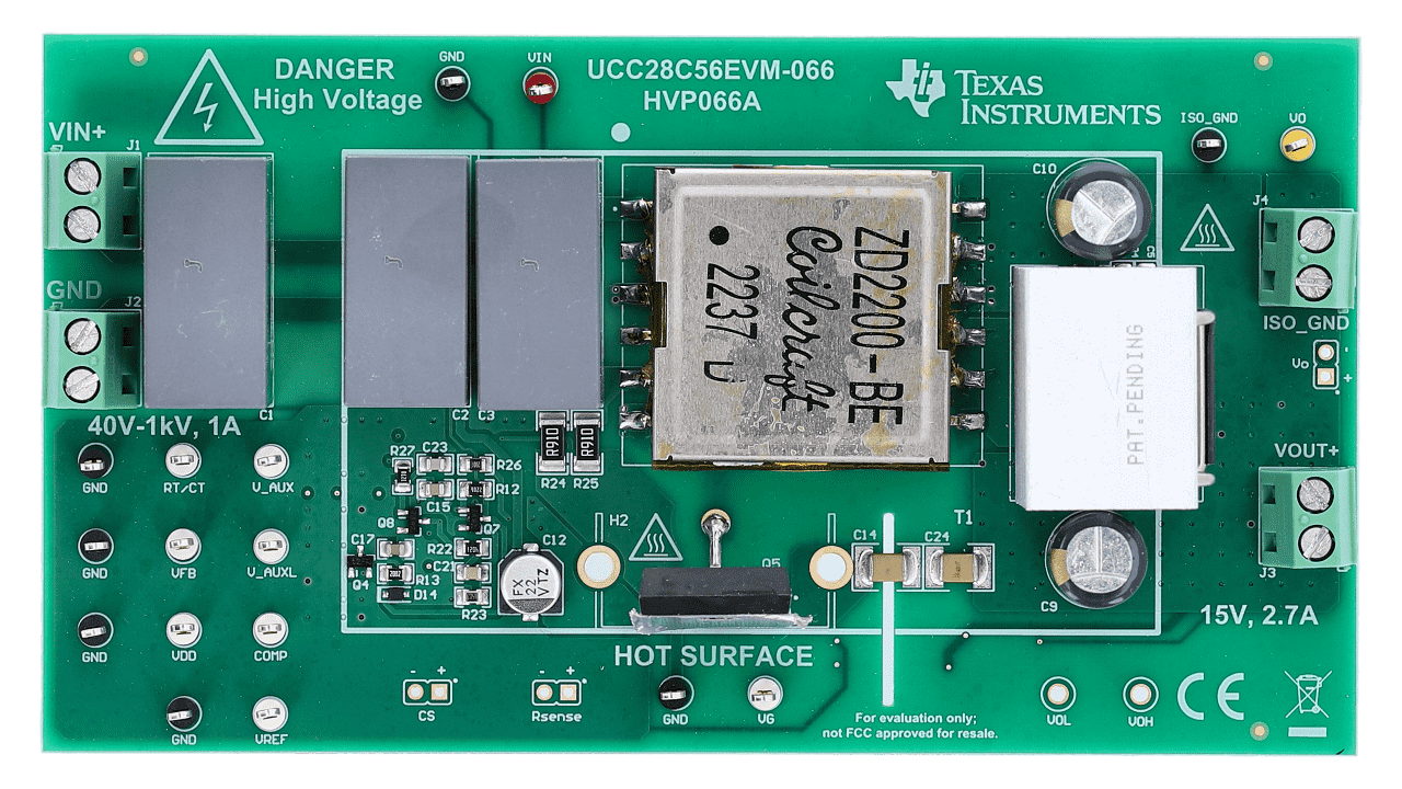
The UCC28C56EVM-066 is a highly efficient primary-side controlled (using an AUX winding) flyback auxiliary power supply for EV/HEV automotive power trains. The design provides 15.2-VTYP, 40-W output for 800-V battery systems. It will deliver 40 W over the input voltage range from 125 V to 1000 V. The exact output voltage is load dependent. From 40-V to 125-V input the design will supply 20 W. The EVM utilizes a 1700-V silicon-carbide (SiC) MOSFET, making it ideal for 800-V battery systems.
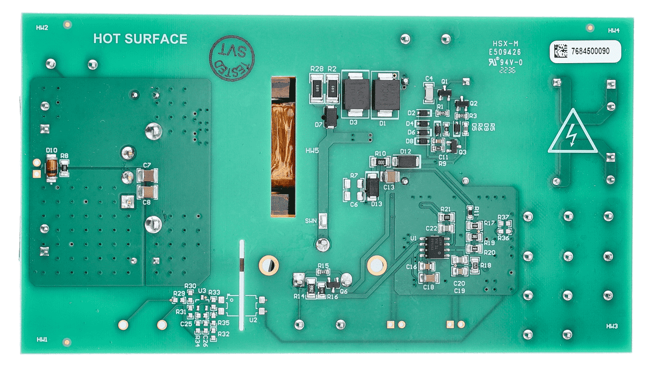
The EVM is a 4-layer board with the top and bottom layers dedicated to signal and power routing. The two inner layers are used only to route test points. In effect, this is a low-cost two-layer PCB. The controller and it's associated power components are tightly compacted into a 50 mm x 86 mm area, highlighted by the white rectangle show on the top silkscreen. Note, C1 is not included with the critical components because it's considered to be part of the general VIN bypass capacitors in the system.
Every effort was made to use automotive qualified components. An automotive qualified 1700-V SiC MOSFET is listed in the BOM. The flyback transformer should be automotive qualified with consultation from the given transformer manufacturer.
 Figure 2-1 UCC28C56EVM-066, HVP066A, Top
View
 Figure 2-2 UCC28C56EVM-066, HVP066A,
Bottom View