SLVA469D June 2013 – January 2023 TLV62130 , TLV62130A , TLV62150 , TLV62150A , TPS61175 , TPS61175-Q1 , TPS62130 , TPS62130A , TPS62131 , TPS62132 , TPS62133 , TPS62135 , TPS62136 , TPS62140 , TPS62140A , TPS62141 , TPS62142 , TPS62143 , TPS62150 , TPS62150A , TPS62151 , TPS62152 , TPS62153 , TPS62160 , TPS62161 , TPS62162 , TPS62163 , TPS62170 , TPS62171 , TPS62172 , TPS62173
2.2 Additional Input Capacitor
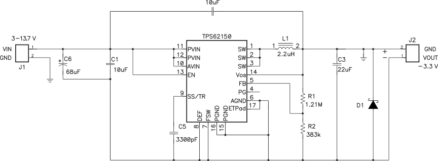
An additional input capacitor, CBYP, is required for stability as a bypass capacitor for the device. This capacitor is in addition to the input capacitor, CIN, from VIN to ground (refer to Figure 1-2). The recommended minimum value for the bypass capacitor and the input capacitor is 10 μF.
As a side effect, the CBYP capacitor provides an AC path from VIN to VOUT. When VIN is applied to the circuit, this dV/dt across a capacitor from VIN to VOUT creates a current that must return to ground (the return of the input supply) to complete its loop. This current might flow through the internal low-side MOSFET's body diode and the inductor to return to ground. Flowing through the body diode pulls the SW pin and VOS pin more than 0.3 V below IC ground, violating their absolute maximum rating. Such a condition might damage the device and is not recommended. Therefore, a Schottky diode should be installed on the output, per Figure 2-3. Startup testing should be conducted to ensure that the VOS pin is not driven more than 0.3 V below IC ground when VIN is applied.
 Figure 2-3 TPS62150 Inverting Buck-boost Schematic with Schottky D1
The AC path through CBYP might also worsen the line transient response. If strong line transients are expected, the output capacitance should be increased to keep the output voltage within acceptable levels during the line transient.