SLVA959B November 2018 – October 2021 DRV10866 , DRV10963 , DRV10964 , DRV10970 , DRV10974 , DRV10975 , DRV10983 , DRV10983-Q1 , DRV10987 , DRV11873 , DRV3205-Q1 , DRV3220-Q1 , DRV3245E-Q1 , DRV3245Q-Q1 , DRV8301 , DRV8302 , DRV8303 , DRV8304 , DRV8305 , DRV8305-Q1 , DRV8306 , DRV8307 , DRV8308 , DRV8312 , DRV8313 , DRV8320 , DRV8320R , DRV8323 , DRV8323R , DRV8332 , DRV8343-Q1 , DRV8350 , DRV8350R , DRV8353 , DRV8353R , DRV8412 , DRV8701 , DRV8702-Q1 , DRV8702D-Q1 , DRV8703-Q1 , DRV8703D-Q1 , DRV8704 , DRV8711 , DRV8800 , DRV8801 , DRV8801-Q1 , DRV8801A-Q1 , DRV8802 , DRV8802-Q1 , DRV8803 , DRV8804 , DRV8805 , DRV8806 , DRV8811 , DRV8812 , DRV8813 , DRV8814 , DRV8816 , DRV8818 , DRV8821 , DRV8823 , DRV8823-Q1 , DRV8824 , DRV8824-Q1 , DRV8825 , DRV8828 , DRV8829 , DRV8830 , DRV8832 , DRV8832-Q1 , DRV8833 , DRV8833C , DRV8834 , DRV8835 , DRV8836 , DRV8837 , DRV8837C , DRV8838 , DRV8839 , DRV8840 , DRV8841 , DRV8842 , DRV8843 , DRV8844 , DRV8846 , DRV8847 , DRV8848 , DRV8850 , DRV8860 , DRV8870 , DRV8871 , DRV8871-Q1 , DRV8872 , DRV8872-Q1 , DRV8873-Q1 , DRV8880 , DRV8881 , DRV8884 , DRV8885 , DRV8886 , DRV8886AT , DRV8889-Q1
7.7 Useful Tools (Net Ties and Differential Pairs)
Many modern CAD tools implement features that can help the layout engineer correctly route the PCB. The features described in this section are part of the Altium Designer tool; however, many other tools have similar features.
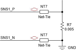
When routing a PCB during the initial stages, the guides that help show which component routes where can be deceptive in the case of the sense resistor routing. In the case of the low-side shunt resistor, the negative input could direct straight to ground, and the positive input could direct to the low-side source pin. To avoid this situation, place a Net Tie between the device and the shunt resistor so that the designer can place the route restriction during placement instead of during routing. Figure 7-6 shows an example of Net Tie placement.
 Figure 7-6 Net Tie Placement Example
The layout technique of using differential pairs reduces common-mode noise by routing two tightly coupled signals in parallel. TI recommends using a differential pair to route the signals from the shunt resistor to the CSA. To reduce noise coupling further, do not route noise-sensitive traces parallel to noisy (switching) signals.