SLVA997A November 2018 – July 2021 TPS61322
1 Traditional Power-Save Mode Control Scheme
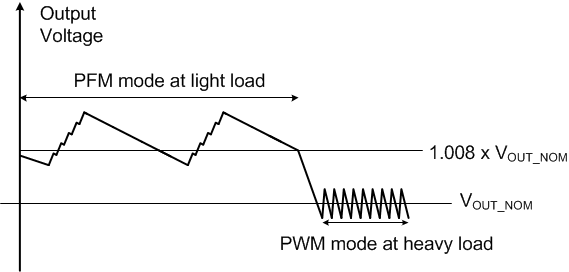
The traditional power-save mode use a low power voltage comparator to enable and disable the control loop under light load. When the output voltage reaches the target value, all the internal blocks will be disabled except the voltage comparator and reference voltage. It is fundamentally a burst-mode-control topology. In systems whose output load is at the boundary of power save mode and normal PWM mode, the device can turn on and off the control loop a number of times. To minimize the probability of the device switch between these two modes, a high hysteresis is added. Then DC output voltage is higher than the nominal value in such kind of control schemes. Typically, the DC voltage in power save mode is 0.5% to 3% higher than the nominal value. Take the TPS61021A as the example, Figure 1-1 is the typical operation behaviors of TPS61021A at light load.
 Figure 1-1 Traditional Power Save Mode
Control Scheme
Figure 1-1 Traditional Power Save Mode
Control SchemeWhen the output load decreases, the error amplifier output is clamped at a certain level. Then the output voltage increases and the devices enters power save mode. During the switching period, the control loop is active and continue to output switching signals until the output voltage hits the PFM reference voltage (0.8% percent higher than the nominal voltage). Then the control loop commands the device stopping switching but actually the device will continue to switch for some cycles because of the internal comparator delay. After that, the device stops switching finally. During the non-switching period, the load is supplied by the output capacitor and the output voltage declines. When the FB voltage drops below the PFM reference voltage, the device starts switching again to ramp up the output voltage after some delay time of the comparator,.
This control scheme is very simple and effective, but it introduces high output ripple because of the multiple switching pulses in one power save mode cycle.