SLVAEE9A October 2019 – July 2021 TPS2065C , TPS2065D , TPS2069C , TPS2069D , TPS25221
1 Introduction
The power-distribution switch family is intended for applications such as USB where heavy capacitive loads and short circuits are likely to be encountered. Device features include enable, reverse blocking when disabled, output discharge pulling down, over-current protection, over temperature protection, and de-glitch fault reporting.
The open-drain output fault signal asserts as over current and over temperature conditions encountered with about 9 ms de-glitch time.
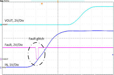
However, as the device is powered up in a fast slew rate, the fault signal falsely asserts that lead to the incorrect operation of the System-on-Chip (SoC). Figure 1-1 shows the set-up of the bench and ramp VIN at 6 V/ms slew rate. Figure 1-2 shows the fault will have a glitch as VIN ramp to about 1 V, which is far from the recommended operation range from 4.5 V to 5.5 V. Table 1-1 is the recommended operating condition of VIN.
 Figure 1-1 Bench Set-Up
 Figure 1-2 Fault
Glitch as Ramp VIN at 6 V/ms
Figure 1-2 Fault
Glitch as Ramp VIN at 6 V/ms| MIN | MAX | UNIT | |
|---|---|---|---|
| VIN Input voltage, IN | 4.5 | 5.5 | V |
The following section discusses the root cause of this phenomenon and the solve method of this concern.