SLVAEX9B April 2022 – August 2022 ESD122 , ESD1LIN24-Q1 , ESD204 , ESD224 , ESD2CAN24-Q1 , ESD2CANFD24 , ESD2CANXL24-Q1 , ESD321 , ESD341 , ESD351 , ESD401 , ESD451 , ESD751 , ESD751-Q1 , ESD752 , ESD761 , ESD761-Q1 , ESD762 , ESDS302 , ESDS304 , ESDS312 , ESDS314 , SN65220 , SN65240 , TPD1E01B04 , TPD1E01B04-Q1 , TPD1E04U04 , TPD1E05U06 , TPD1E05U06-Q1 , TPD1E0B04 , TPD1E10B06 , TPD1E10B09-Q1 , TPD1E1B04 , TPD1E6B06 , TPD2E001 , TPD2E001-Q1 , TPD2E007 , TPD2E009 , TPD2E1B06 , TPD2E2U06 , TPD2EUSB30 , TPD2EUSB30A , TPD2S017 , TPD3E001 , TPD3F303 , TPD4E001 , TPD4E001-Q1 , TPD4E002 , TPD4E004 , TPD4E02B04 , TPD4E02B04-Q1 , TPD4E05U06-Q1 , TPD4E101 , TPD4E110 , TPD4E1B06 , TPD4E1U06 , TPD4E6B06 , TPD4F003 , TPD4S009 , TPD4S012 , TPD5E003 , TPD6E001 , TPD6E004 , TPD6E05U06 , TPD8S009 , TSD05 , TSD05C , TSM24A-Q1 , TSM24CA-Q1 , TSM36A , TVS0500 , TVS0701 , TVS1400 , TVS1401 , TVS2200 , TVS2701 , TVS3301 , UC1611-SP , UC2610 , UC3610 , UC3611 , UC3611M
- Abstract
- Trademarks
- 1Definitions of ESD Device Specifications
- 2ESD Layout Tips
-
3ESD Solutions by Package Types
- 3.1 0201 2-pin SON (TI: DPL) | 0.6 mm x 0.3 mm
- 3.2 0402 2-pin SON (TI: DPY) | 1.0 mm × 0.6 mm
- 3.3 2-pin SOD-523 (TI: DYA) | 1.2 mm x 0.8 mm
- 3.4 3-pin SOT-9X3 (TI: DRT) | 1 mm × 1 mm
- 3.5 3-pin SC70 (TI: DCK) | 2 mm × 1.25 mm
- 3.6 3-pin SOT23 (TI:DBZ) | 3.04 mm × 2.64 mm
- 3.7 4-pin SON (TI: DPW) | 0.8 mm × 0.8 mm
- 3.8 5-pin SOT-5X3 (TI: DRL) | 1.6 mm × 1.2 mm
- 3.9 5-pin SOT-23 (TI: DBV) | 2.9 mm × 1.6 mm
- 3.10 6-pin SON (TI: DRY) | 1.45 mm × 1 mm
- 3.11 6-pin SOT-5X3 (TI: DRL) | 1.6 mm × 1.2 mm
- 3.12 6-pin SOT-23 (TI: DBV) | 1.6 mm × 2.9 mm
- 3.13 6-pin SC70 (TI: DCK) | 2.15 mm × 1.4 mm
- 3.14 8-pin SON (TI: DQD) | 1.35 mm × 1.7 mm
- 3.15 10-pin SON (TI: DQA) | 1 mm × 2.5 mm
- 4References
- 5Revision History
2.4 Optimizing Ground Schemes for ESD
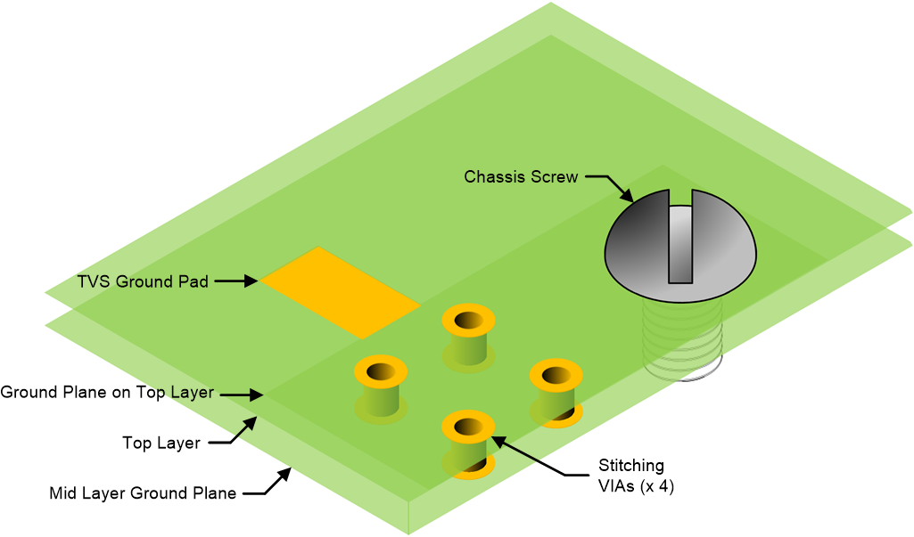
For TVS, having a very low impedance path to ground is very important. Eliminating all the parasitic inductances between the ESD source and the TVS will only be effective if the TVS is optimally grounded. Figure 2-4 shows the ground pad of a TVS connected to the top layer ground plane.
 Figure 2-4 Two Layer PCB -
Top Ground Plane Stitched to a Mid-layer Ground
Plane
Figure 2-4 Two Layer PCB -
Top Ground Plane Stitched to a Mid-layer Ground
PlaneThe TVS ground pin should connect to a same layer ground plane that is coupled with another ground plane on an immediately adjacent layer. These ground planes should be stitched together with VIAs, with one VIA immediately adjacent to the ground pin of the TVS. Use the following tips to optimize the grounding scheme with very low impedance:
- Connect the TVS ground pin directly to a same layer ground plane that has nearby VIAs stitching to an adjacent internal ground plane
- Use multiple ground planes when possible
- Use a grounded chassis screw to connect the PCB ground and position it near the TVS and ESD source as the connector ground shield
- Use VIAs of large diameter with a large drill, which lowers impedance
For more detailed explanations, see the ESD Protection Layout Guide Application Report.