SLVAF46A May 2021 – January 2023 TPS65988
2.6 Test Setup and Results
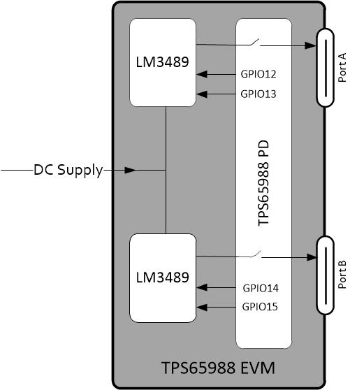
The control logic to balance port power (as shown in Figure 2-6) can be tested on TPS65988EVM using the project file. TPS65988EVM has two Buck regulators (LM3489) corresponding to Port A and Port B as shown in Figure 2-13. The GPIO pins GPIO12 and GPIO13 are mapped to output GPIO events Port 0 Source PDO Negotiated TT1 and Port 0 Source PDO Negotiated TT2 events, respectively. These GPIOs toggle based on the negotiated PDO and set the feedback voltage of LM3489 accordingly, to generate the negotiated PDO voltage. Similarly, voltage on Port B (Port 1) is controlled by GPIO14 and GPIO15. In the actual application, Buck regulators shall be replaced by ACDC and DCDC regulators as shown in Figure 2-13. TPS65988DH includes three I2C ports out of which one I2C port can work as both master and slave, one I2C port can work as a I2C master only and one can work as a I2C slave only. The I2C masters allow the PD controller to control various kinds of slaves directly based on events inside the PD controller. I2C master events can be used to configure ACDC/DCDC with I2C interface.
 Figure 2-13 EVM Block Diagram
Following are the steps to prepare EVM and then test the port power balancing control logic.
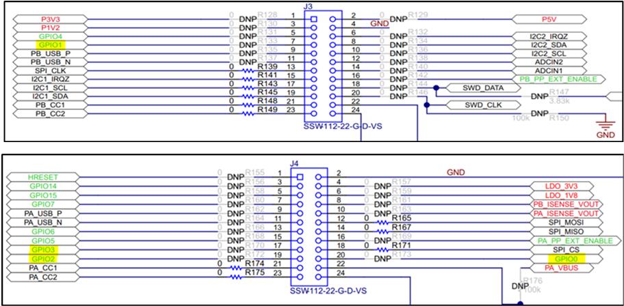
- Populate 0E resistors R170-R173 and R133 to make GPIO0-GPIO3 signals available on signal headers J3 and J4.
- Short GPIO0 (on J4) to GPIO1 (on J3) and GPIO2
(on J4) to GPIO3 (on J4) using jumper wires.
 Figure 2-14 GPIO Setting on
EVM
 - Populate PPHV jumpers to connect buck regulators' outputs to the system side of internal power switches. Short pins 5-7 and 6-8 of J11.
- Power up the EVM by connecting the Power Adapter to barrel Jack connector J1.
- Load the project file in GUI Software tool and load the firmware patch in PD controller.
- Power cycle the EVM by unplugging and plugging the Power Adapter.
- Connect a PD capable Sink device to one of the ports through a PD analyzer. The TPS665988DH Source port must advertise 60W capability; ensure the same by checking the Source Capability message.
- Connect another PD device to the second port and verify that the already connected port advertises modified 30W Source Capability message.
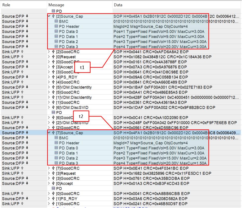
Figure 2-15 shows the PD trace captured on Port 0. At t1 – only Port 0 is connected and therefore the source capability message shows 60W. At t2 – Port 1 is also connected and therefore Port 0 scaled down its power capability to 30W. The modified 30W source cap message transmitted from Port 0 at t2 is also show in the figure.
 Figure 2-15 PD Trace Showing PDOs
Corresponding to Single and Dual Port Connections
Figure 2-15 PD Trace Showing PDOs
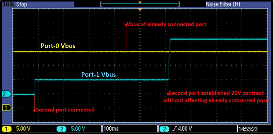
Corresponding to Single and Dual Port ConnectionsFigure 2-16 shows Port-0 (channel 1) and Port-1 (Channel 2) Vbus voltage transitions captured in parallel with the PD trace. Channel 2 shows Port-1 Vbus transition to 20 V.
 Figure 2-16 Scope Capture of Vbus Transitions