SLVS350K October 2002 – June 2025 TPS795
PRODUCTION DATA
- 1
- 1 Features
- 2 Applications
- 3 Description
- 4 Pin Configuration and Functions
- 5 Specifications
- 6 Detailed Description
- 7 Application and Implementation
- 8 Device and Documentation Support
- 9 Revision History
- 10Mechanical, Packaging, and Orderable Information
4 Pin Configuration and Functions
 Figure 4-1 DRB Package, 8-Pin VSON
(Top View, Legacy Chip)
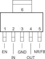
 Figure 4-3 DCQ Package, 6-Pin SOT-223
(Top View, Legacy Chip)
Figure 4-3 DCQ Package, 6-Pin SOT-223
(Top View, Legacy Chip)Figure 4-2 DRB Package, 8-Pin VSON
(Top View, New Chip)
Figure 4-4 DCQ Package, 6-Pin SOT-223
(Top View, New Chip)
Table 4-1 Pin Functions
| PIN | TYPE | DESCRIPTION | ||
|---|---|---|---|---|
| NAME | VSON | SOT-223 | ||
| EN | 8 | 1 | I | Driving the enable pin (EN) high turns on the regulator. Driving this pin low puts the regulator into shutdown mode. EN can be connected to IN if not used. |
| FB | 5 | 5 | I | Feedback input voltage for the adjustable device. |
| GND | 6 | 3, 6 | — | Regulator ground |
| IN | 1, 2 | 2 | I | Input to the device. |
| N/C | 5,7 | 5 | — | No internal connection |
| NR | 5 | 5 | — | Legacy chip: Noise-reduction pin for fixed versions only. Connecting an external capacitor to this pin bypasses noise generated by the internal band gap, which improves power-supply rejection and reduces output noise.(Not available on adjustable versions.) For lower noise performance device, consider the TPS7A90. |
| OUT | 3, 4 | 4 | O | Regulator output |
| Thermal Pad | Pad | — | — | Connect the thermal pad to a large-area ground plane. The thermal pad is internally connected to GND. |