SLVS561O December   2004  – June 2025 TLV1117

PRODUCTION DATA  

  1.   1
  2. Features
  3. Applications
  4. Description
  5. Pin Configuration and Functions
  6. Specifications
    1. 5.1 Absolute Maximum Ratings
    2. 5.2 ESD Ratings
    3. 5.3 Recommended Operating Conditions
    4. 5.4 Thermal Information (Legacy Chip)
    5. 5.5 Thermal Information (New Chip)
    6. 5.6 Electrical Characteristics
    7. 5.7 Typical Characteristics
  7. Detailed Description
    1. 6.1 Overview
    2. 6.2 Functional Block Diagrams
    3. 6.3 Feature Description
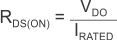
      1. 6.3.1 Dropout Voltage (Fixed Output, New Chip)
      2. 6.3.2 Foldback Current Limit (Fixed Output, New Chip)
      3. 6.3.3 Undervoltage Lockout (Fixed Output, New Chip)
      4. 6.3.4 Thermal Shutdown (Fixed Output, New Chip)
      5. 6.3.5 Load Regulation (Adjustable Output, New Chip)
    4. 6.4 Device Functional Modes
      1. 6.4.1 Device Functional Mode Comparison (Fixed Output, New Chip)
      2. 6.4.2 Normal Operation (Fixed Output)
      3. 6.4.3 Dropout Operation (Fixed Output, New Chip)
      4. 6.4.4 Protection Diodes (Adjustable Output, New Chip)
  8. Application and Implementation
    1. 7.1 Application Information
      1. 7.1.1 Recommended Capacitor Types (Fixed Output, New Chip)
      2. 7.1.2 Input and Output Capacitor Requirements (Fixed Output, New Chip)
      3. 7.1.3 Reverse Current (Fixed Output, New Chip)
      4. 7.1.4 Power Dissipation (Fixed Output, New Chip)
      5. 7.1.5 Estimating Junction Temperature (Fixed Output, New Chip)
    2. 7.2 Typical Application (Adjustable Output)
      1. 7.2.1 Design Requirements (Adjustable Output)
      2. 7.2.2 Detailed Design Procedure
        1. 7.2.2.1 Detailed Design Procedure (Fixed Output, New Chip)
        2. 7.2.2.2 Detailed Design Procedure (Adjustable Output)
      3. 7.2.3 Application Curves
    3. 7.3 Power Supply Recommendations
    4. 7.4 Layout
      1. 7.4.1 Layout Guidelines
      2. 7.4.2 Layout Example
  9. Device and Documentation Support
    1. 8.1 Device Support
      1. 8.1.1 Device Nomenclature
    2. 8.2 Receiving Notification of Documentation Updates
    3. 8.3 Support Resources
    4. 8.4 Trademarks
    5. 8.5 Electrostatic Discharge Caution
    6. 8.6 Glossary
  10. Revision History
  11. 10Mechanical, Packaging, and Orderable Information

Dropout Voltage (Fixed Output, New Chip)

Dropout voltage (VDO) is defined as VIN – VOUT at the rated output current (IRATED), where the pass transistor is fully on. VIN is the input voltage, VOUT is the output voltage, and IRATED is the maximum IOUT listed in the Recommended Operating Conditions table. At this operating point, the pass transistor is driven fully on. Dropout voltage indirectly specifies a minimum input voltage greater than the nominal programmed output voltage where the output voltage is expected to stay in regulation. If the input voltage falls to less than the nominal output regulation, then the output voltage falls as well.

For a CMOS regulator, the dropout voltage is determined by the drain-source, on-state resistance (RDS(ON)) of the pass transistor. Therefore, if the linear regulator operates at less than the rated current, the dropout voltage for that current scales accordingly. The following equation calculates the RDS(ON) of the device.

Equation 1. TLV1117