SLVSDR8B April 2018 – February 2023 TPS62147 , TPS62148
PRODUCTION DATA
- 1 Features
- 2 Applications
- 3 Description
- 4 Revision History
- 5 Device Comparison Table
- 6 Pin Configuration and Functions
- 7 Specifications
- 8 Parameter Measurement Information
-
9 Detailed Description
- 9.1 Overview
- 9.2 Functional Block Diagram
- 9.3 Feature Description
- 9.4
Device Functional Modes
- 9.4.1 Pulse Width Modulation (PWM) Operation
- 9.4.2 Power Save Mode Operation (PWM/PFM)
- 9.4.3 100% Duty-Cycle Operation
- 9.4.4 Current Limit And Short Circuit Protection (for TPS62148)
- 9.4.5 HICCUP Current Limit And Short Circuit Protection (for TPS62147)
- 9.4.6 Soft Start / Tracking (SS/TR)
- 9.4.7 Output Discharge Function (TPS62148 only)
- 9.4.8 Starting into a Pre-Biased Load
- 10Application and Implementation
- 11Device and Documentation Support
- 12Mechanical, Packaging, and Orderable Information
6 Pin Configuration and Functions
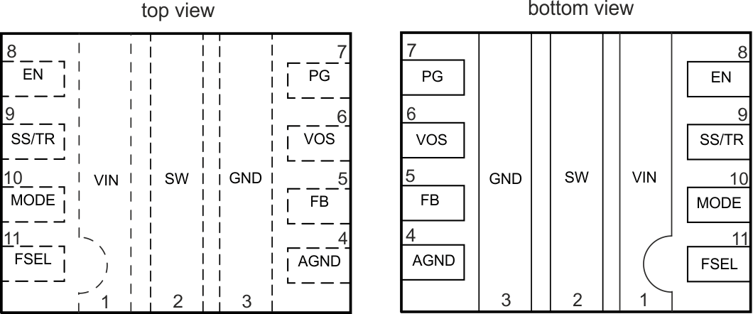
 Figure 6-1 RGX Package11-Pin VQFN
Table 6-1 Pin Functions
| PIN | I/O | DESCRIPTION | |
|---|---|---|---|
| NUMBER | NAME | ||
| 1 | VIN | I | Power supply input. Make sure the input capacitor is connected as close as possible between pin VIN and GND. |
| 2 | SW | Switch pin of the converter connected to the internal Power MOSFETs. | |
| 3 | GND | I | Ground pin. |
| 4 | AGND | I | Connect to GND. |
| 5 | FB | I | Voltage feedback input. Connect resistive output voltage divider to this pin. |
| 6 | VOS | I | Output voltage sense pin. Connect directly to the positive pin of the output capacitor. |
| 7 | PG | O | Open drain power good output. Leave open or tie to GND if not used. |
| 8 | EN | I | Enable pin of the device. Connect to logic low to disable the device. Pull high to enable the device. Do not leave this pin unconnected. |
| 9 | SS/TR | I | Soft-start / Tracking pin. An external capacitor connected from this pin to GND defines the rise time for the internal reference voltage. The pin can also be used as an input for tracking and sequencing - see Detailed Description section in this document. |
| 10 | MODE | I | The device runs in PFM/PWM mode when this pin is pulled low. When the pin is pulled high, the device runs in forced PWM mode. Do not leave this pin unconnected. |
| 11 | FSEL | I | Switching frequency setting pin. Pull to logic low for a switching frequency of 1.25 MHz. Pull to logic high for a switching frequency of 2.5 MHz. Do not leave FSEL unconnected. |