SLVUA85A June 2014 – May 2021 TPS65261
3.1 EVM Layout
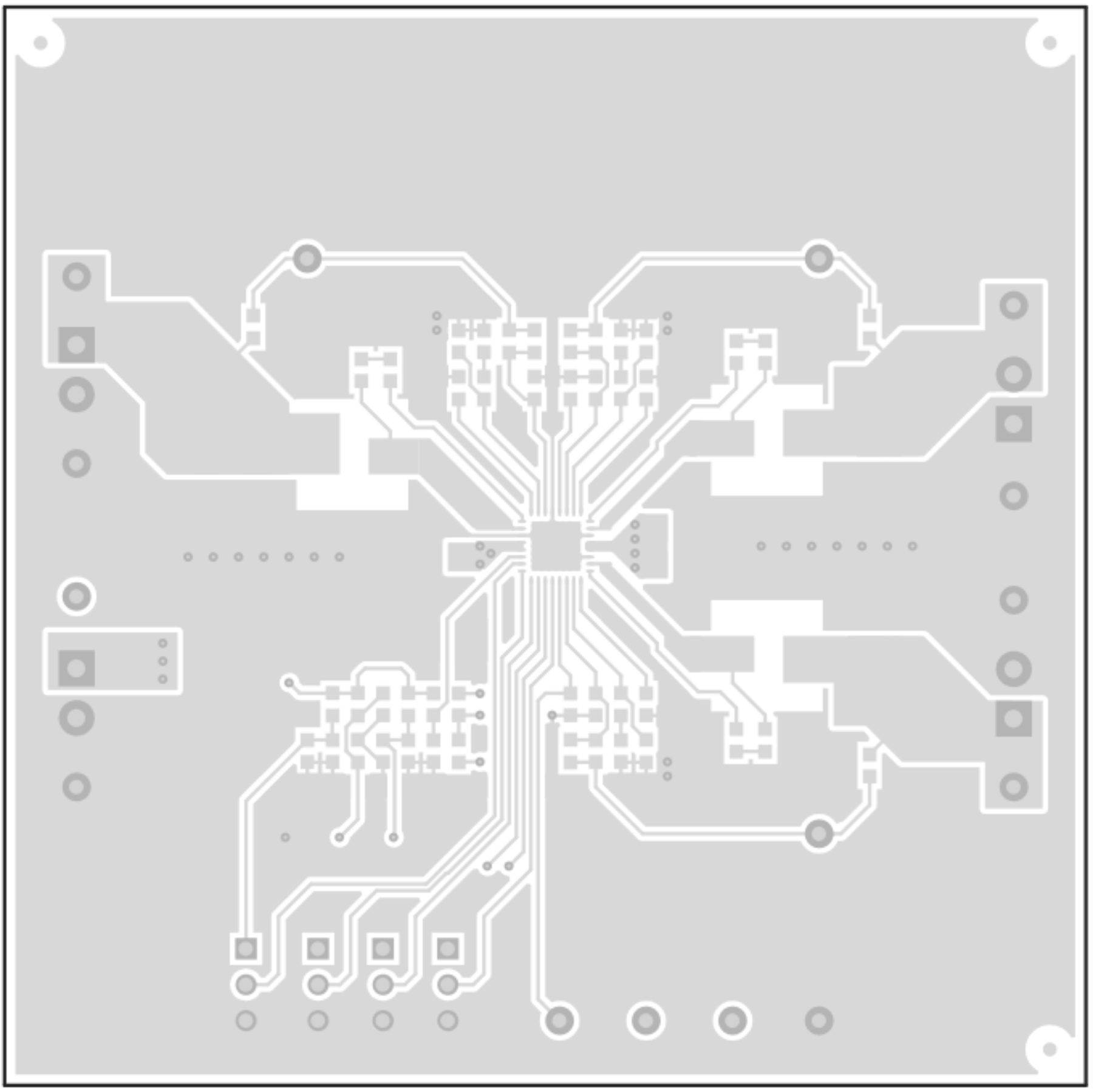
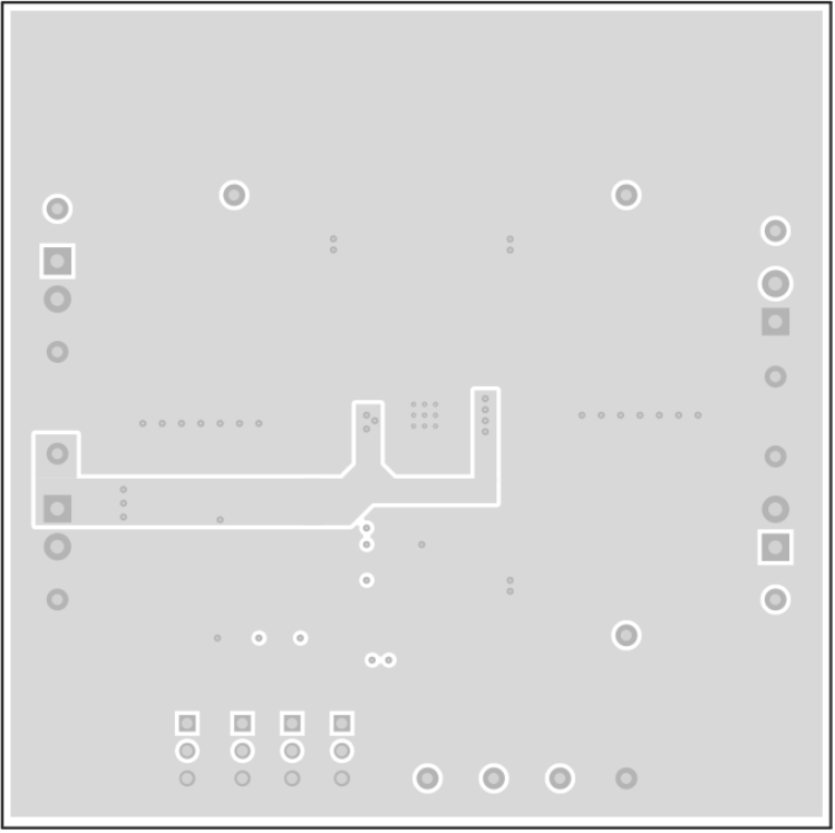
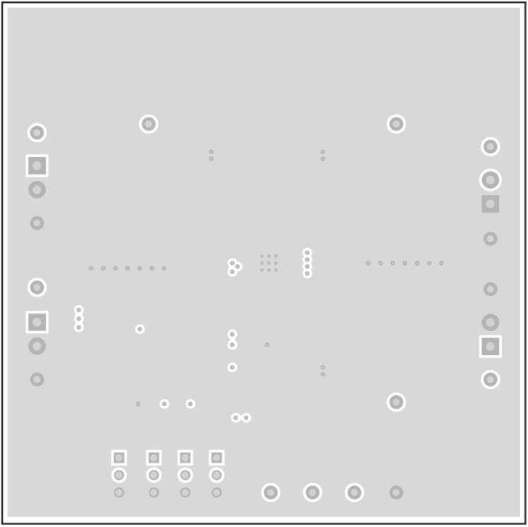
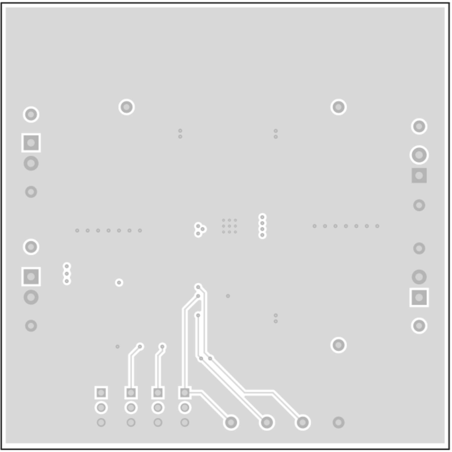
Figure 3-2 through Figure 3-5 illustrate the PCB layout for this EVM.
 Figure 3-2 Board Layout (Top Layer)
 Figure 3-4 Board Layout (Third Layer)
 Figure 3-3 Board Layout (Second Layer)
 Figure 3-5 Board Layout (Bottom Layer)