SLVUBX2A August 2020 – March 2021 TPS62912 , TPS62913
1.2.6 Loop Response Measurement
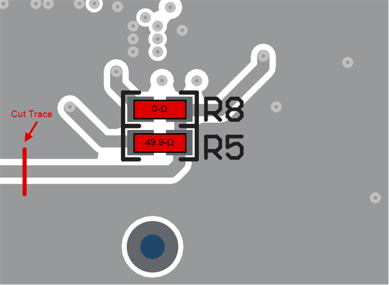
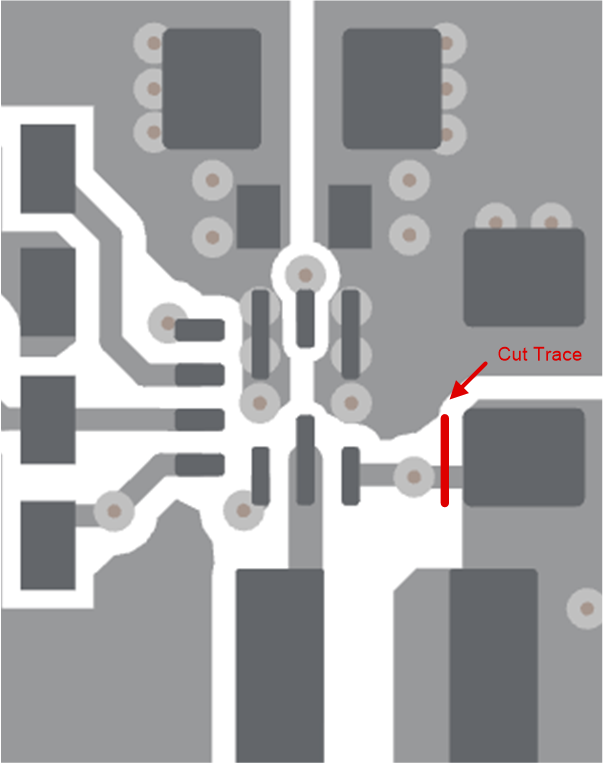
The loop response can be measured with simple changes to the circuitry. First, install a 49.9-Ω resistor across R5's pads on the back of the PCB and install a 0-Ω resistor across R8's pads on the back of the PCB. The pads are spaced to allow installation of a 0603-sized resistors. Second, cut the trace on the bottom layer below the added 49.9-Ω resistor. Figure 1-1 shows these changes. Third, cut the short section of trace on the top layer between the via on pin 3 and C4. Figure 1-2 shows this change. Lastly, replace the ferrite bead (FB1) with a 0-Ω resistor. The second LC filter must be removed to break the complete feedback loop and measure the loop response. With these changes, an AC signal (10-mV, peak-to-peak amplitude recommended) can be injected into the control loop across the added 49.9-Ω resistor. Figure 3-2 shows the results of this test.
 Figure 1-1 Loop Response Measurement Modification
(Bottom Layer).
  Figure 1-2 Loop Response
Measurement Modification (Top Layer).