SLVUC32B June 2021 – February 2022 DRA829J , DRA829J-Q1 , DRA829V , DRA829V-Q1 , TDA4VM , TDA4VM-Q1 , TPS6594-Q1
- Trademarks
- 1Introduction
- 2Device Versions
- 3Processor Connections
- 4Supporting Functional Safety Systems
-
5Static NVM Settings
- 5.1 Application-Based Configuration Settings
- 5.2 Device Identification Settings
- 5.3 BUCK Settings
- 5.4 LDO Settings
- 5.5 VCCA Settings
- 5.6 GPIO Settings
- 5.7 Finite State Machine (FSM) Settings
- 5.8 Interrupt Settings
- 5.9 POWERGOOD Settings
- 5.10 Miscellaneous Settings
- 5.11 Interface Settings
- 5.12 Multi-Device Settings
- 5.13 Watchdog Settings
- 6Pre-Configurable Finite State Machine (PFSM) Settings
- 7Impact of NVM Changes
- 8References
- 9Revision History
6.3.7 TO_MCU
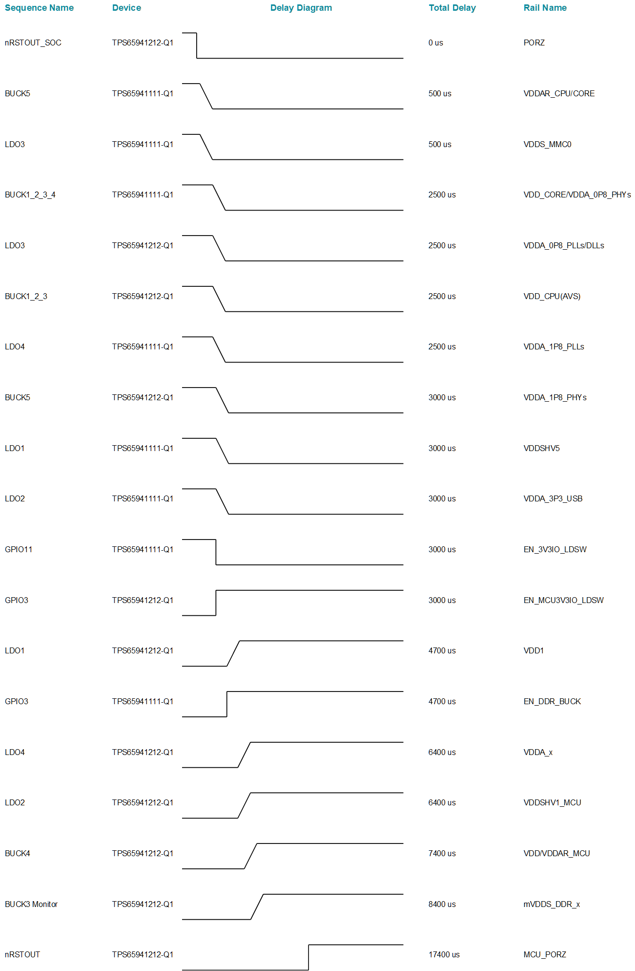
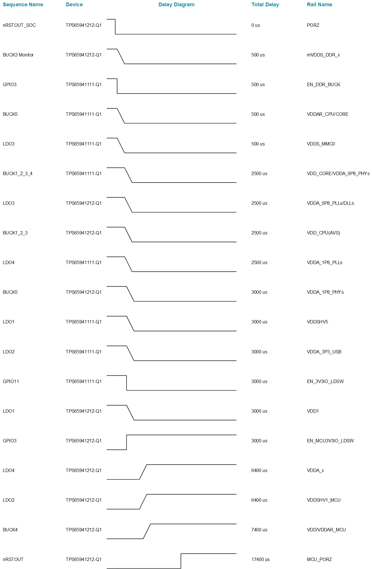
The TO_MCU sequence first turns off rails and GPIOs which are assigned to the SOC power group. The sequence then enables the MCU rails, in the event that they are not already active (when transitioning from STANDBY to MCU_ONLY for example). There are two cases for this sequence, based off the value stored in the I2C_7 register bit of primary TPS65941212-Q1. If the bit is low, then VDD1, EN_DDR_BUCK and mVDDS_DDR_x, are disabled; Figure 6-9. If the I2C_7 bit is high, then VDD1, EN_DDR_BUCK and mVDDS_DDR_x are enabled; Figure 6-10.
The first instructions of the TO_MCU sequence perform writes to the MISC_CTRL and ENABLE_DRV_STAT registers.
// TPS65941212Q1
// Set AMUXOUT_EN, CLKMON_EN
// Clear LPM_EN, NRSTOUT_SOC
REG_WRITE_MASK_IMM ADDR=0x81 DATA=0x18 MASK=0xE1
// Clear SPMI_LP_EN
REG_WRITE_MASK_IMM ADDR=0x82 DATA=0x00 MASK=0xEF
// TPS65941111Q1
// Set AMUXOUT_EN, CLKMON_EN
// Clear LPM_EN
REG_WRITE_MASK_IMM ADDR=0x81 DATA=0x18 MASK=0xE3
// Clear SPMI_LP_EN
REG_WRITE_MASK_IMM ADDR=0x82 DATA=0x00 MASK=0xEF
 Figure 6-9 TO_MCU with I2C_7 HIGH; VDD1
is Unchanged in Sequence
 Figure 6-10 TO_MCU with I2C_7 LOW, VDD1 is
Disabled in Sequence
Figure 6-10 TO_MCU with I2C_7 LOW, VDD1 is
Disabled in SequenceThe last instructions of the TO_MCU sequence also perform writes to the MISC_CTRL and ENABLE_DRV_STAT registers after the delay defined in the PFSM_DELAY_REG_1.
// TPS65941212Q1
SREG_READ_REG ADDR=0xCD REG=R1
DELAY_SREG R1
// Clear SPMI_LPM_EN and FORCE_EN_DRV_LOW
REG_WRITE_MASK_IMM ADDR=0x82 DATA=0x00 MASK=0xE7
// Set NRSTOUT (MCU_PORZ)
REG_WRITE_MASK_IMM ADDR=0x81 DATA=0x01 MASK=0xFE