SLVUC32B June 2021 – February 2022 DRA829J , DRA829J-Q1 , DRA829V , DRA829V-Q1 , TDA4VM , TDA4VM-Q1 , TPS6594-Q1
- Trademarks
- 1Introduction
- 2Device Versions
- 3Processor Connections
- 4Supporting Functional Safety Systems
-
5Static NVM Settings
- 5.1 Application-Based Configuration Settings
- 5.2 Device Identification Settings
- 5.3 BUCK Settings
- 5.4 LDO Settings
- 5.5 VCCA Settings
- 5.6 GPIO Settings
- 5.7 Finite State Machine (FSM) Settings
- 5.8 Interrupt Settings
- 5.9 POWERGOOD Settings
- 5.10 Miscellaneous Settings
- 5.11 Interface Settings
- 5.12 Multi-Device Settings
- 5.13 Watchdog Settings
- 6Pre-Configurable Finite State Machine (PFSM) Settings
- 7Impact of NVM Changes
- 8References
- 9Revision History
3.1 Power Mapping
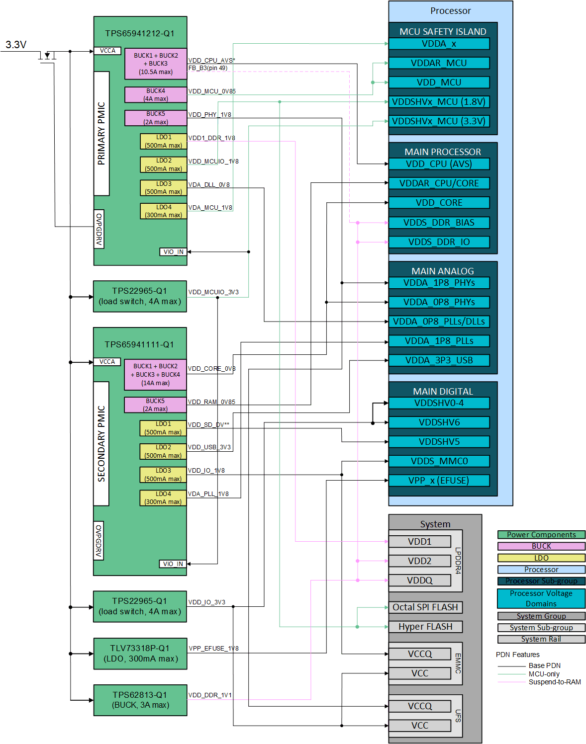
Figure 3-1 shows the power mapping between the dual TPS6594-Q1 PMIC power resources and processor voltage domains required to support independent MCU and Main power rails. In this configuration, both PMICs use a 3.3 V input voltage. For Functional Safety applications, there is a protection FET before VCCA that connects to the OVPGDRV pin of the primary PMIC, allowing voltage monitoring of the input supply to the PMICs.
The VCCA voltage must be the first voltage applied to the PMIC devices. VIO_IN of the PMICs must not be supplied before VCCA. A load switch supplies VIO_IN in this PDN. This load switch also supplies the VDDSHVx_MCU voltage domain of the processor. This allows PMIC GPIO control signals referenced to VIO_IN to remain active during MCU Only low power mode and to be disabled during DDR Retention (aka Suspend-to-RAM) to reduce PMIC power.
For SD card dual-voltage I/O support (3.3 V and 1.8 V), LDO1 of the TPS659411-Q1 device can be used. A processor GPIO control signal with a logic high default value is used to set SD VIO to 3.3 V initially. During processor power up, the boot loader SW can set GPIO signal low to select 1.8 V level as needed for high-speed card operation per SD specification. This allows control of the LDO1 voltage without the need for the MCU processor to establish I2C communication with the PMICs during boot from SD card operations.
This PDN uses four discrete power components with three being required and one is optional depending upon end product features. The two TPS22965-Q1 Load Switches connect VCCA_3V3 power rail to supply OV protected 3.3 V to processor I/O domains. Two load switches are required in order to enable isolation between MCU and Main processor sub-sections for MCU Safety Island or MCU Only low power operations. The TPS62813-Q1 Buck Converter supplies LPDDR4 SDRAM component with required 1.1V supply. The unused primary PMIC FB pin, FB_B3, has been configured per NVM settings, Table 5-3, to provide voltage monitoring for VDD_DDR_1V1 power rail if an end product OV/UV monitoring requirements include this supply. The one optional discrete power component is TLV73318-Q1 LDO that can be used if an end product uses a high security processor type and desires the capability to program Efuse values on-board. If this feature is not desired, then this LDO can be omitted and processor VPP pins treated per data manual recommendations.
 Figure 3-1 Power Connections
- * VDD_CPU_AVS, boot voltage of 0.8 V then software sets device specific AVS; 0.68 V – 0.72 V.
- ** VDD_SD_DV, 3.3 V then software changes to 1.8 V per HS-SD.
Table 3-1 identifies which power resources are required to support different system features. If the system feature listed is not required, the power resource connection can be removed and the processor voltage domains need to be grouped into alternative power rails.
| Power Mapping | System Features | |||||||
|---|---|---|---|---|---|---|---|---|
| Device | Power Resource | Power Rails | Processor and Memory Domains | Active SoC | MCU - only | Suspend-to-RAM | SD Card | USB Interface |
| TPS65941212-Q1 | BUCK123 | VDD_CPU_AVS | VDD_CPU | Required | ||||
| FB_B3 | VDDS_DDR_BIAS, VDDS_DDR_IO, LPDDR4 | Required | Required | |||||
| BUCK4 | VDD_MCU_0V85 | VDDAR_MCU, VDD_MCU | Required | Required | ||||
| BUCK5 | VDD_PHY_1V8 | VDDA_1P8_PHYs | Required | |||||
| LDO1 | VDD1_DDR_1V8 | Mem: VDD1 | Required | Optional | Required | |||
| LDO2 | VDD_MCUIO_1V8 | VDDSHVx_MCU (1.8 V) | Required | Required | ||||
| Mem: VCC | ||||||||
| LDO3 | VDA_DLL_0V8 | VDDA_0P8_PLLs/DLLs | Required | |||||
| LDO4 | VDA_MCU_1V8 | VDDA_x | Required | Required | ||||
| TPS65941111-Q1 | BUCK1234 | VDD_CORE_0V8 | VDD_CORE, VDDA_0P8_PHYs | Required | ||||
| BUCK5 | VDD_RAM_0V85 | VDDAR_CPU/CORE | Required | |||||
| LDO1 | VDD_SD_DV | VDDSHV5 | Required | |||||
| LDO2 | VDD_USB_3V3 | VDDA_3P3_USB | Required | |||||
| LDO3 | VDD_IO_1V8 | VDDS_MMC0 | Required | |||||
| Mem: VCCQ | ||||||||
| LDO4 | VDA_PLL_1V8 | VDDA_1P8_PLLs | Required | |||||
| TPS22965-Q1 | Load Switch | VDD_MCUIO_3V3 | VDDSHVx_MCU (3.3 V) | Required | Required | |||
| TPS22965-Q1 | Load Switch | VDD_IO_3V3 | VDDSHV0-4,VDDSHV6 (3.3 V) | Required | Required | |||
| TLV73318P-Q1 | LDO | VPP_EFUSE_1V8 | VPP_x(EFUSE) | Optional | ||||
| TPS62813-Q1 | BUCK | VDD_DDR_1V1 | VDDS_DDR_BIAS, VDDS_DDR_IO | Required | Optional | Required | ||
| Mem: VDD2 | ||||||||