SLVUC32B June 2021 – February 2022 DRA829J , DRA829J-Q1 , DRA829V , DRA829V-Q1 , TDA4VM , TDA4VM-Q1 , TPS6594-Q1
- Trademarks
- 1Introduction
- 2Device Versions
- 3Processor Connections
- 4Supporting Functional Safety Systems
-
5Static NVM Settings
- 5.1 Application-Based Configuration Settings
- 5.2 Device Identification Settings
- 5.3 BUCK Settings
- 5.4 LDO Settings
- 5.5 VCCA Settings
- 5.6 GPIO Settings
- 5.7 Finite State Machine (FSM) Settings
- 5.8 Interrupt Settings
- 5.9 POWERGOOD Settings
- 5.10 Miscellaneous Settings
- 5.11 Interface Settings
- 5.12 Multi-Device Settings
- 5.13 Watchdog Settings
- 6Pre-Configurable Finite State Machine (PFSM) Settings
- 7Impact of NVM Changes
- 8References
- 9Revision History
3.2 Control Mapping
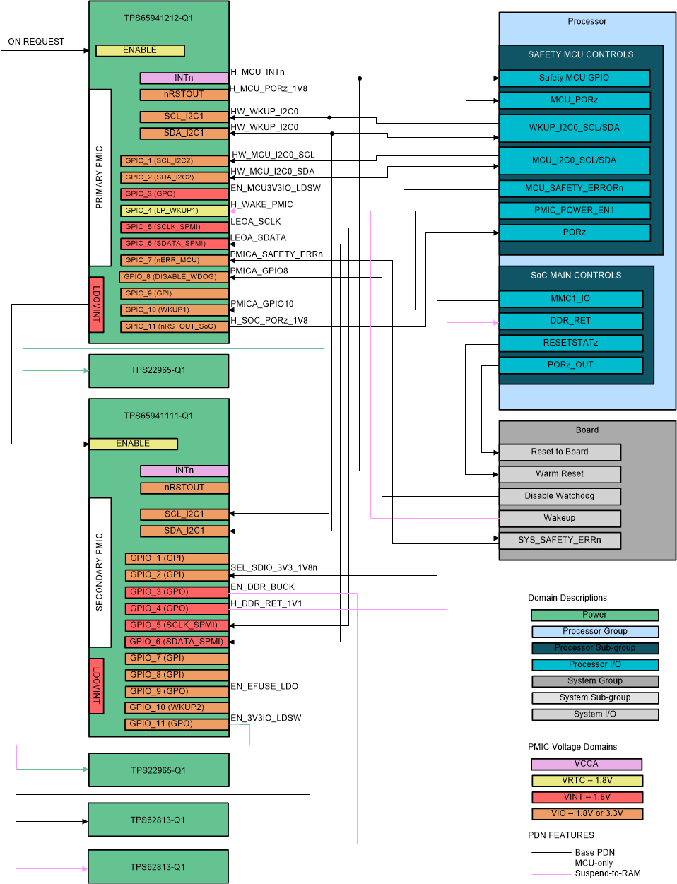
Figure 3-2 shows the digital control signal mapping between processor and PMIC devices. For the two PMIC devices to work together, the primary PMIC and secondary PMIC must establish an SPMI communication channel. This allows the two TPS6594-Q1 to synchronize their internal Pre-Configurable State Machines (PFSM) so that they operate as one PFSM across all power and digital resources. The GPIO_5 and GPIO_6 pins on the TPS6594-Q1 are assigned for this functionality. In addition, the primary PMIC LDOVINT pin is connected to the secondary PMIC ENABLE input to correctly initiate the PFSM.
Other digital connections from the TPS6594-Q1 devices to the processor provide error monitoring, processor reset, processor wake up, and system low-power modes. Specific GPIO pins have been assigned to key signals in order to ensure proper operation during low power modes when only a few GPIO pins remain operational.
The digital connections shown in Figure 3-2 allow system features including MCU-only MCU Safety Island and suspend-to-RAM low power modes, functional safety up to ASIL-D, compliant dual voltage SD card operation, and LPDDR4x integration.
 Figure 3-2 TPS6594-Q1 Digital
Connections
Figure 3-2 TPS6594-Q1 Digital
Connections| PDN Signal | Pullup Power Rail |
|---|---|
| H_MCU_INTn | VDD_MCUIO_3V3 |
| H_MCU_PORz_1V8 | VDA_MCU_1V8 |
| H_SOC_PORz_1V8 | VDA_MCU_1V8 |
| H_DDR_RET_1V1 | VDD_DDR_1V1_REG |
| H_WKUP_I2C0 | VDD_MCUIO_3V3 |
| H_MCU_I2C0_SCL/SDA | VDD_MCUIO_3V3 |
Please use Table 3-3 as a guide to understand GPIO assignments required for each PDN system feature. If the feature listed is not required, the digital connection can be removed; however, the GPIO pin is still configured per NVM defined default function shown. After the processor has booted up, system software can potentially reconfigure an unused GPIO to support a new function. This is possible as long as that function is only needed after boot and default function does not cause any conflicts with normal operations (for example, two outputs driving same net). For details on how functional safety related connections help achieve functional safety system-level goals, see Section 4.
| Device | GPIO Mapping | System Features | ||||||
|---|---|---|---|---|---|---|---|---|
| PMIC Pin | NVM Function | PDN Signals | Active SoC | Functional Safety | MCU - only and MCU-Safety Island | Suspend-to-RAM | SD Card | |
| TPS65941212-Q1 | nPWRON/ ENABLE | Enable | SOC_PWR_ON | Required | ||||
| INT | INT | H_MCU_INTn | Required | |||||
| nRSTOUT | nRSTOUT | H_MCU_PORz_1V8 | Required | Required | ||||
| SCL_I2C1 | SCL_I2C1 | H_WKUP_I2C0 | Required | |||||
| SDA_I2C1 | SDA_I2C1 | H_WKUP_I2C0 | Required | |||||
| GPIO_1 | SCL_I2C2 | H_MCU_I2C0_SCL | Required | |||||
| GPIO_2 | SDA_I2C2 | H_MCU_I2C0_SDA | Required | |||||
| GPIO_3 | GPO | EN_MCU3V3IO_LDSW | Required | |||||
| GPIO_4 | LP_WKUP1 | H_WAKE_PMIC | Required | |||||
| GPIO_5 | SCLK_SPMI | LEOA_SCLK | Required | |||||
| GPIO_6 | SDATA_SPMI | LEOA_SDATA | Required | |||||
| GPIO_7 | nERR_MCU | PMICA_SAFETY_ERRn | Required | |||||
| GPIO_8 | DISABLE_WDOG | PMICA_GPIO8 | (2) | (2) | ||||
| GPIO_9 | GPI | PMICA_GPIO9(3) | ||||||
| GPIO_10 | WKUP1 | PMIC_POWER_EN1 | Required | |||||
| GPIO_11 | nRSTOUT_SOC | H_SOC_PORz_1V8 | Required | |||||
| TPS65941111-Q1 | nPWRON/ENABLE | ENABLE | VINT_LEOA_1V8 | Required | ||||
| nINT | nINT | H_MCU_INTn | ||||||
| nRSTOUT | nRSTOUT | Unused | ||||||
| SCL_I2C1 | SCL_I2C1 | H_WKUP_I2C0 | Required | |||||
| SDA_I2C1 | SCL_I2C1 | H_WKUP_I2C0 | Required | |||||
| GPIO_1 | GPI | Unused(3) | ||||||
| GPIO_2 | GPI | SEL_SDIO_3V3_1V8n(1) | Required | |||||
| GPIO_3 | GPO | EN_DDR_BUCK | ||||||
| GPIO_4 | GPO | H_DDR_RET_1V1 | Required | |||||
| GPIO_5 | SCLK_SPMI | LEOA_SCLK | Required | |||||
| GPIO_6 | SDATA_SPMI | LEOA_SDATA | Required | |||||
| GPIO_7 | GPI | Unused(3) | ||||||
| GPIO_8 | GPI | Unused(3) | ||||||
| GPIO_9 | GPO | EN_EFUSE_LDO(3) | ||||||
| GPIO_10 | WKUP2 | Unused(3) | ||||||
| GPIO_11 | GPO | EN_3V3IO_LDSW | Required | |||||