SLVUCA4 August   2021 TPS1653


  1.   Trademarks
  2. 1Introduction
    1. 1.1 REACH Compliance
    2. 1.2 EVM Features
    3. 1.3 Applications
  3. 2Description
  4. 3General Configurations
    1. 3.1 Physical Access
    2. 3.2 Test Equipment
      1. 3.2.1 Power Supplies
      2. 3.2.2 Meters
      3. 3.2.3 Oscilloscope
      4. 3.2.4 Loads
    3. 3.3 Test Setup
    4. 3.4 Test Procedure
      1. 3.4.1 Preliminary Tests
      2. 3.4.2 UVLO Tests
      3. 3.4.3 Current Limit Test with Step Load of 4 A to 7 A
      4. 3.4.4 Output Short-Circuit Protection Test
      5. 3.4.5 Start-Up With Short-Circuit On Output
  5. 4EVM Board Assembly Drawings and Layout
    1. 4.1 PCB Drawings
  6. 5Schematics
  7. 6Bill of Materials

PCB Drawings

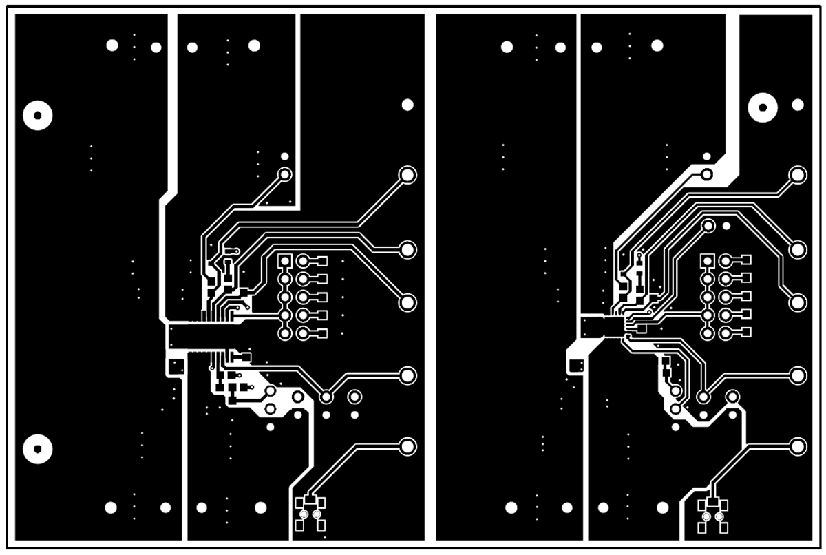
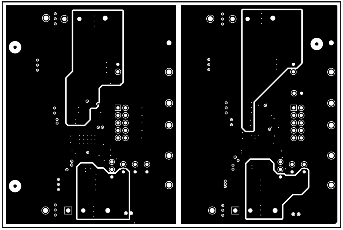
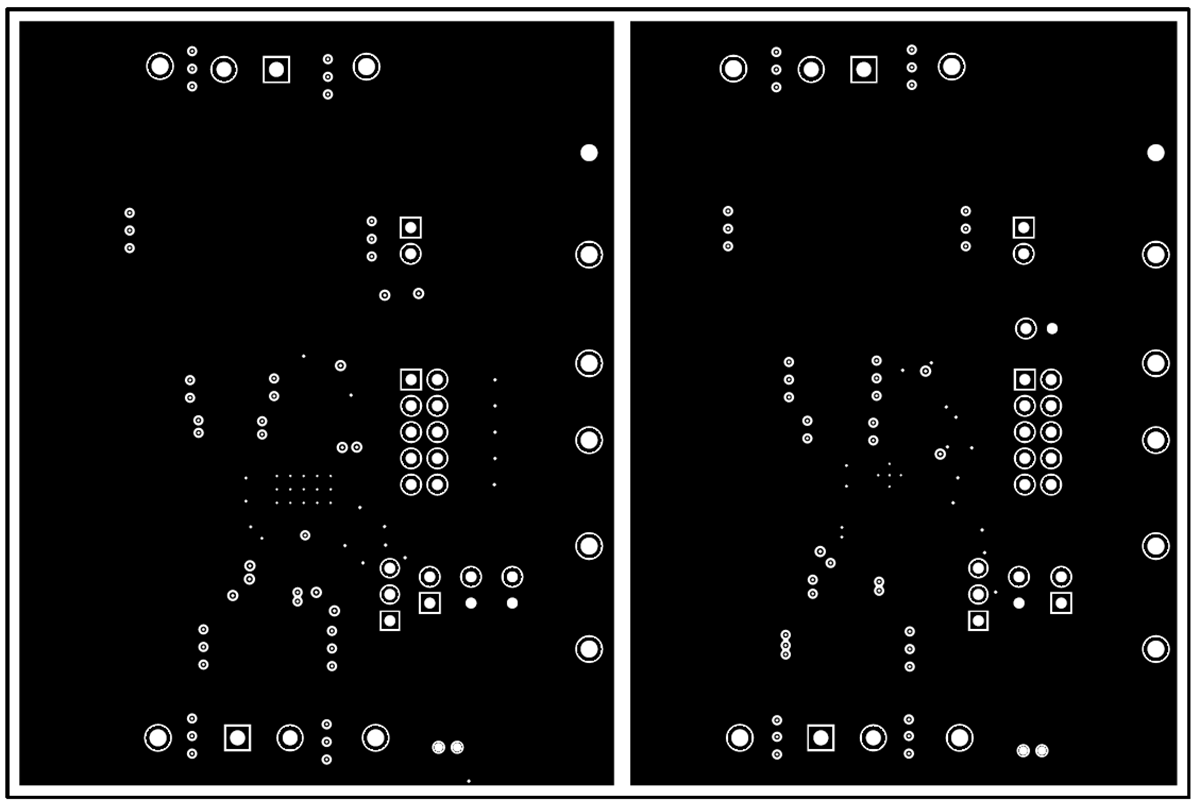
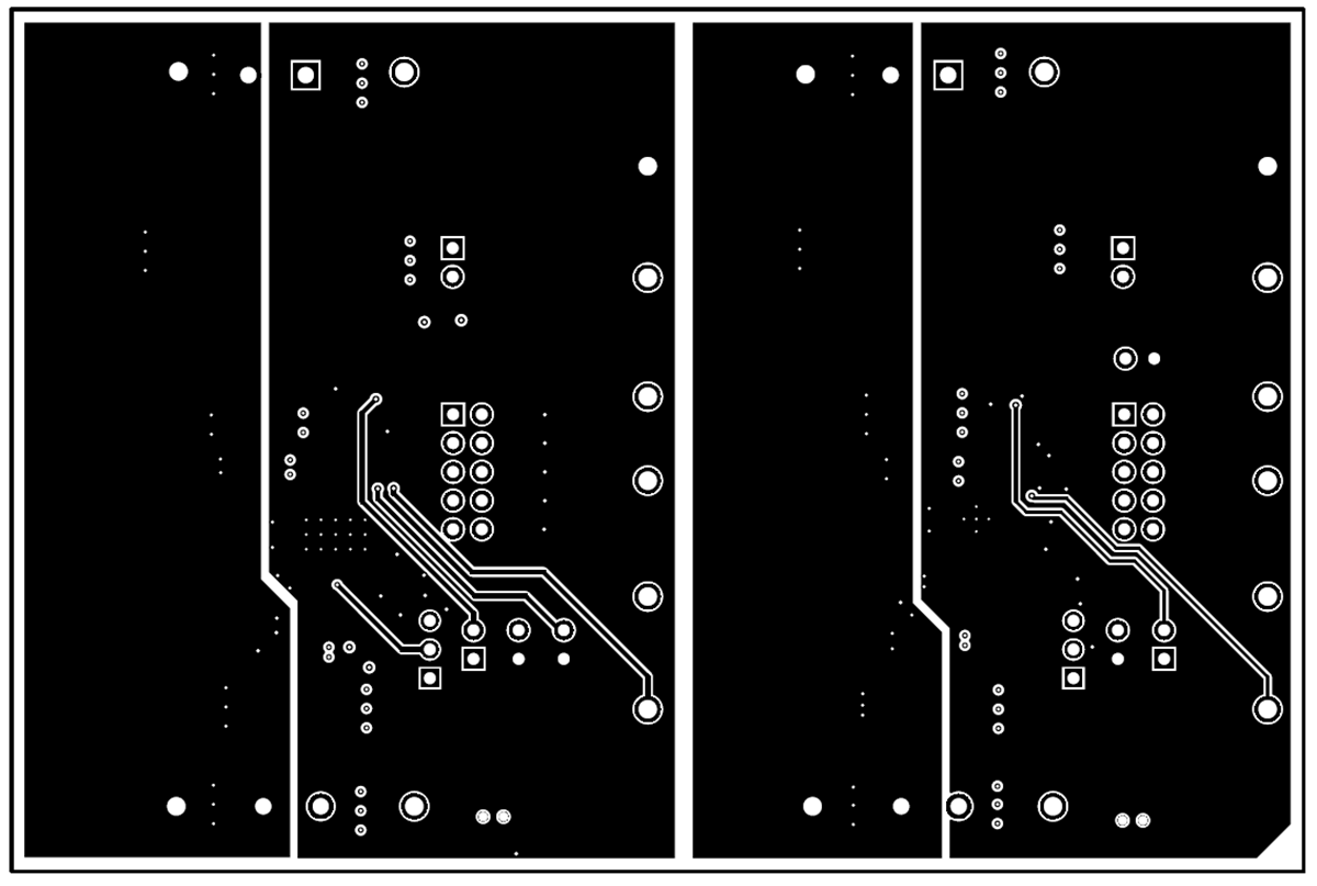
Figure 4-1 through Figure 4-3 show component placement and layout of the EVM.
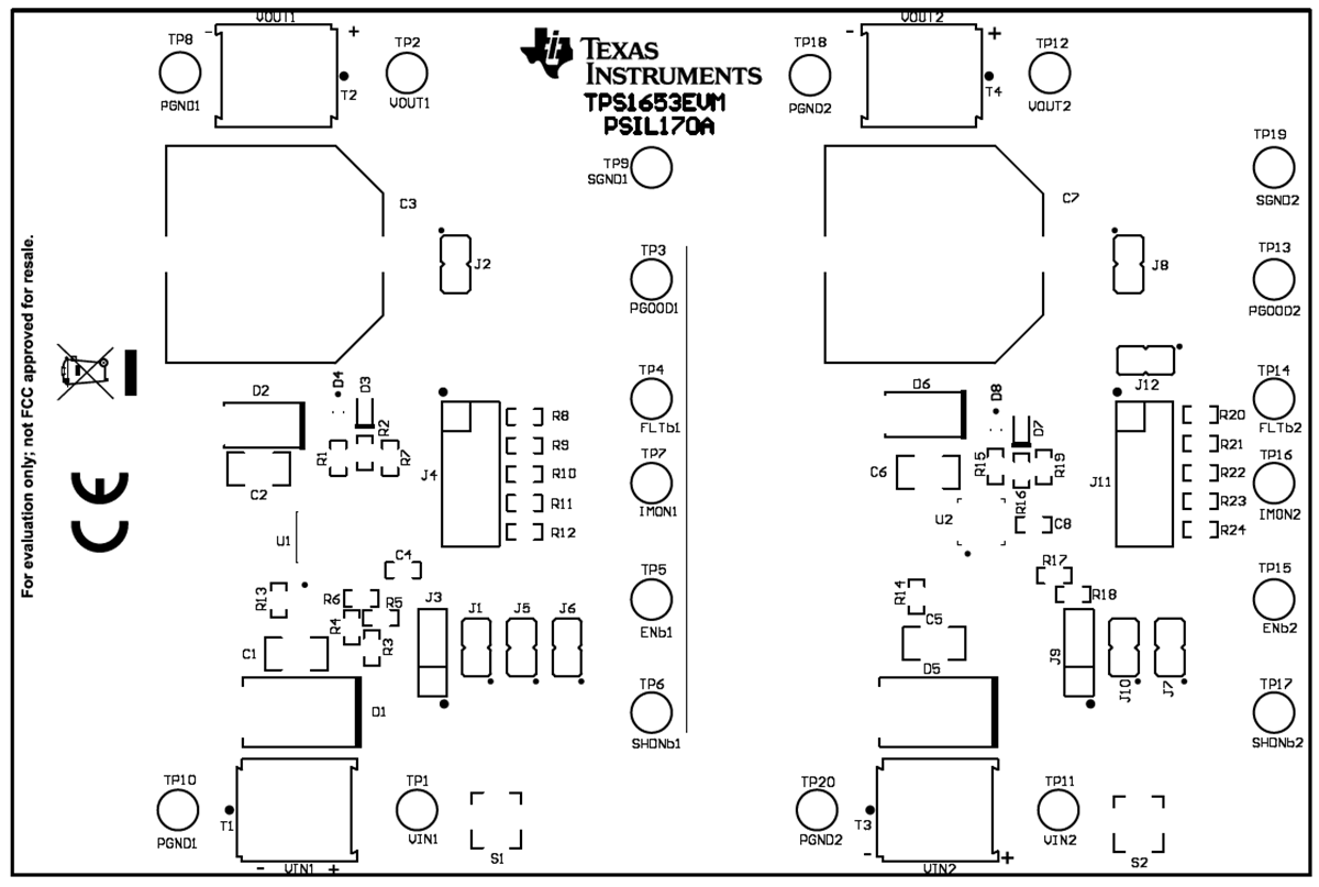
GUID-20210811-SS0I-8NKM-RF77-DTGCT2S65QN0-low.pngFigure 4-1 Top Side Placement
GUID-20210811-SS0I-PXFG-XXZP-D24KQS8HHG2W-low.pngFigure 4-2 Top Layer
GUID-20210811-SS0I-TSCV-KG9D-WV4866CN29M8-low.pngFigure 4-3 Bottom Layer
GUID-20210809-SS0I-90BR-HZD9-SCKC41X41GCP-low.png Figure 4-4 Inner Ground Layer
GUID-20210809-SS0I-4TLZ-SDDH-SRBLZCDMCFC5-low.png Figure 4-5 Inner Routing Layer