SNAS717A April 2017 – October 2021 ADC12D1620QML-SP
PRODUCTION DATA
- 1 Features
- 2 Applications
- 3 Description
- 4 Revision History
- 5 Pin Configuration and Functions
-
6 Specifications
- 6.1 Absolute Maximum Ratings
- 6.2 ESD Ratings
- 6.3 Recommended Operating Conditions
- 6.4 Thermal Information
- 6.5 Converter Electrical Characteristics: Static Converter Characteristics
- 6.6 Converter Electrical Characteristics: Dynamic Converter Characteristics
- 6.7 Converter Electrical Characteristics: Analog Input/Output and Reference Characteristics
- 6.8 Converter Electrical Characteristic: Channel-to-Channel Characteristics
- 6.9 Converter Electrical Characteristics: LVDS CLK Input Characteristics
- 6.10 Electrical Characteristics: AutoSync Feature
- 6.11 Converter Electrical Characteristics: Digital Control and Output Pin Characteristics
- 6.12 Converter Electrical Characteristics: Power Supply Characteristics
- 6.13 Converter Electrical Characteristics: AC Electrical Characteristics
- 6.14 Electrical Characteristics: Delta Parameters
- 6.15 Timing Requirements: Serial Port Interface
- 6.16 Timing Requirements: Calibration
- 6.17 Quality Conformance Inspection
- 6.18 Timing Diagrams
- 6.19 Typical Characteristics
-
7 Detailed Description
- 7.1 Overview
- 7.2 Functional Block Diagram
- 7.3 Feature Description
- 7.4 Device Functional Modes
- 7.5
Programming
- 7.5.1
Control Modes
- 7.5.1.1
Non-ECM
- 7.5.1.1.1 Dual-Edge Sampling Pin (DES)
- 7.5.1.1.2 Non-Demultiplexed Mode Pin (NDM)
- 7.5.1.1.3 Dual Data-Rate Phase Pin (DDRPh)
- 7.5.1.1.4 Calibration Pin (CAL)
- 7.5.1.1.5 Low-Sampling Power-Saving Mode Pin (LSPSM)
- 7.5.1.1.6 Power-Down I-Channel Pin (PDI)
- 7.5.1.1.7 Power-Down Q-Channel Pin (PDQ)
- 7.5.1.1.8 Test-Pattern Mode Pin (TPM)
- 7.5.1.1.9 Full-Scale Input-Range Pin (FSR)
- 7.5.1.1.10 AC- or DC-Coupled Mode Pin (VCMO)
- 7.5.1.1.11 LVDS Output Common-Mode Pin (VBG)
- 7.5.1.2 Extended Control Mode
- 7.5.1.1
Non-ECM
- 7.5.1
Control Modes
- 7.6 Register Maps
- 8 Application Information Disclaimer
- 9 Power Supply Recommendations
- 10Layout
- 11Device and Documentation Support
- 12Mechanical, Packaging, and Orderable Information
11.1.1 Device Nomenclature
APERTURE (SAMPLING) DELAY is the amount of delay, measured from the sampling edge of the CLK input, after which the signal present at the input pin is sampled inside the device.
APERTURE JITTER (tAJ) is the variation in aperture delay from sample-to-sample. Aperture jitter can be effectively considered as noise at the input.
CODE ERROR RATE (CER) is the probability of error and is defined as the probable number of word errors on the ADC output per unit of time divided by the number of words seen in that amount of time. A CER of 10–18 corresponds to a statistical error in one word about every 31.7 years for the adc12d1620QML-SP .
CLOCK DUTY CYCLE is the ratio of the time that the clock waveform is at a logic high to the total time of one clock period.
DIFFERENTIAL NON-LINEARITY (DNL) is the measure of the maximum deviation from the ideal step size of 1 LSB. It is measured at the relevant sample rate, fCLK, with fIN = 1 MHz sine wave.
EFFECTIVE NUMBER OF BITS (ENOB, or EFFECTIVE BITS) is method of specifying signal-to-noise and distortion ratio, or SINAD. ENOB is defined as (SINAD − 1.76) / 6.02 and states that the converter is equivalent to a perfect ADC of this many (ENOB) number of bits.
GAIN ERROR is the deviation from the ideal slope of the transfer function. It can be calculated from offset and full-scale errors. the positive gain error is the offset error minus the positive full-scale error. The negative gain error is the negative full-scale error minus the offset error. The gain error is the negative full-scale error minus the positive full-scale error; it is also equal to the positive gain error plus the negative gain error.
GAIN FLATNESS is the measure of the variation in gain over the specified bandwidth. For example, for the adc12d1620QML-SP, from D.C. to Fs/2 is to 800 MHz for the non-DES mode and from D.C. to Fs/2 is 1600 MHz for the DES mode.
INTEGRAL NON-LINEARITY (INL) is a measure of worst-case deviation of the ADC transfer function from an ideal straight line drawn through the ADC transfer function. The deviation of any given code from this straight line is measured from the center of that code value step. The best fit method is used.
INSERTION LOSS is the loss in power of a signal due to the insertion of a device, for example the adc12d1620, expressed in dB.
INTERMODULATION DISTORTION (IMD) is a measure of the near-in 3rd order distortion products (2f2 – f1, 2f1 – f2), which occur when two tones that are close in frequency (f1, f2) are applied to the ADC input. It is measured from the input tone's level to the higher of the two distortion products (dBc) or simply the level of the higher of the two distortion products (dBFS).
LSB (LEAST SIGNIFICANT BIT) is the bit that has the smallest value or weight of all bits. This value is
where
- VFS is the differential full-scale amplitude VIN_FSR as set by the FSR input
- N is the ADC resolution in bits, which is 12 for the adc12d1620
LOW VOLTAGE DIFFERENTIAL SIGNALING (LVDS) DIFFERENTIAL OUTPUT VOLTAGE (VID and VOD) is two times the absolute value of the difference between the VD+ and VD- signals; each signal measured with respect to ground. VOD peak is VOD,P= (VD+ – VD–) and VOD peak-to-peak is VOD,P-P= 2 × (VD+ – VD–); for this product, the VOD is measured peak-to-peak.
 Figure 11-1 LVDS Output Signal Levels
LVDS OUTPUT OFFSET VOLTAGE (VOS) is the midpoint between the D+ and D– pins output voltage with respect to ground; that is , [(VD+) +( VD-)]/2. See Figure 11-1.
MISSING CODES are those output codes that are skipped and will never appear at the ADC outputs. These codes cannot be reached with any input value.
MSB (MOST SIGNIFICANT BIT) is the bit that has the largest value or weight. Its value is one half of full scale.
NEGATIVE FULL-SCALE ERROR (NFSE) is a measure of how far the first code transition is from the ideal 1/2 LSB above a differential −VIN / 2 with the FSR pin low. For the adc12d1620 the reference voltage is assumed to be ideal, so this error is a combination of full-scale error and reference voltage error.
NOISE FLOOR DENSITY is a measure of the power density of the noise floor, expressed in dBFS/Hz and dBm/Hz. '0 dBFS' is defined as the power of a sinusoid that precisely uses the full-scale range of the ADC.
NOISE POWER RATIO (NPR) is the ratio of the sum of the power inside the notched bins to the sum of the power in an equal number of bins outside the notch, expressed in dB.
OFFSET ERROR (VOFF) is a measure of how far the mid-scale point is from the ideal zero voltage differential input.
Offset Error = Actual Input causing average of 8 k samples to result in an average code of 2047.5.
OUTPUT DELAY (tOD) is the time delay (in addition to latency) after the rising edge of CLK+ before the data update is present at the output pins.
OVER-RANGE RECOVERY TIME is the time required after the differential input voltages goes from ±1.2 V to 0 V for the converter to recover and make a conversion with its rated accuracy.
PIPELINE DELAY (LATENCY) is the number of input clock cycles between initiation of conversion and when that data is presented to the output driver stage. The data lags the conversion by the latency plus the tOD.
POSITIVE FULL-SCALE ERROR (PFSE) is a measure of how far the last code transition is from the ideal 1-1/2 LSB below a differential +VIN / 2. For the ADC12D1620 the reference voltage is assumed to be ideal, so this error is a combination of full-scale error and reference voltage error.
SIGNAL-TO-NOISE RATIO (SNR) is the ratio, expressed in dB, of the rms value of the fundamental for a single-tone to the rms value of the sum of all other spectral components below one-half the sampling frequency, not including harmonics or DC.
SIGNAL-TO-NOISE PLUS DISTORTION (S/(N+D) or SINAD) is the ratio, expressed in dB, of the rms value of the fundamental for a single tone to the rms value of all of the other spectral components below half the input clock frequency, including harmonics but excluding DC.
SPURIOUS-FREE DYNAMIC RANGE (SFDR) is the difference, expressed in dB, between the rms values of the input signal at the output and the peak spurious signal, where a spurious signal is any signal present in the output spectrum that is not present at the input, excluding DC.
RθJA is the thermal resistance between the junction to ambient.
RθJB is the thermal resistance between the junction and the circuit board close to the outer pins.
RθJT is the thermal resistance between the junction and the case, measured at the lid of the package.
TOTAL HARMONIC DISTORTION (THD) is the ratio expressed in dB, of the rms total of the first nine harmonic levels at the output to the level of the fundamental at the output. THD is calculated as
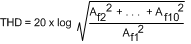
where
- Af1 is the RMS power of the fundamental (output) frequency
- Af2 through Af10 are the RMS power of the first 9 harmonic frequencies in the output spectrum
– Second Harmonic Distortion (2nd Harm) is the difference, expressed in dB, between the RMS power in the input frequency seen at the output and the power in its 2nd harmonic level at the output.
– Third Harmonic Distortion (3rd Harm) is the difference expressed in dB between the RMS power in the input frequency seen at the output and the power in its 3rd harmonic level at the output.