SNAU252 June 2020 LMK04832-SP
- LMK04832EVM-CVAL User’s Guide
- A TICS Pro Usage
2.1.1 Clock Outputs Page Description
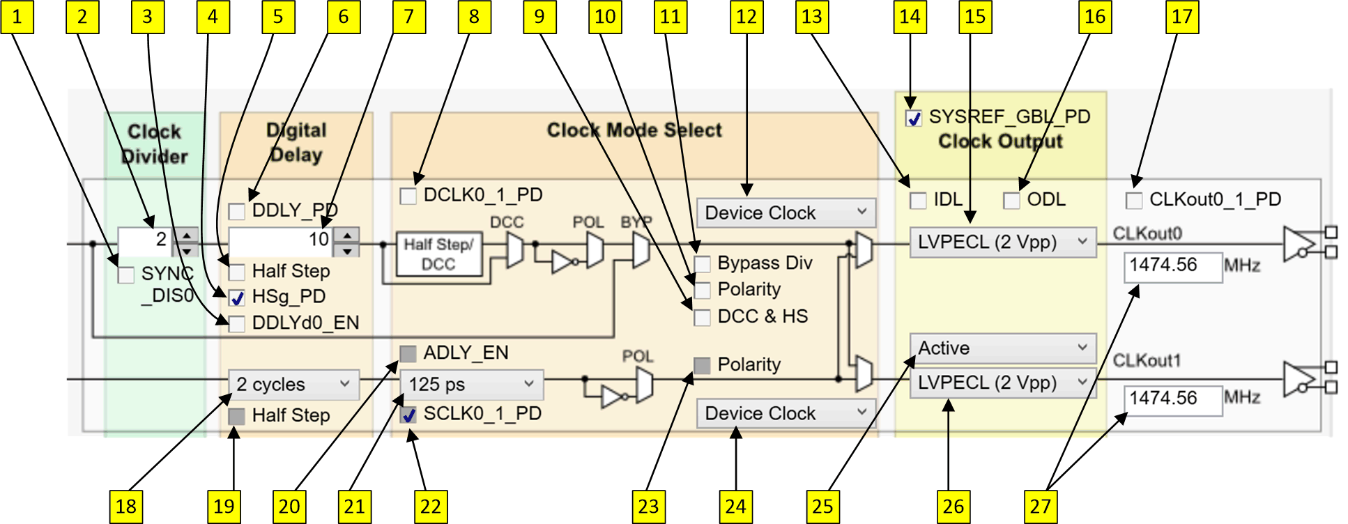
Clock outputs are grouped in pairs. This description applies for all clock outputs on the Clock Outputs page of the TICS Pro GUI shown in Section A.9.
 Figure 2. Clock Outputs Page Description Diagram
 - SYNC_DISX: Prevent the divider from being reset by SYNC/SYSREF path.
- DCLKX_Y_DIV: Divide value for the device clock. If set to 1, then DCLKX_Y_DCC (DCC & HS) must = 1.
- DDLYdX_EN: Enable dynamic digital delay for this divider.
- DCLKX_Y_HSg_PD: If clear, glitchless half-step adjustments are enabled.
- DCLKX_Y_HS: Set half step for this divider. DCLKX_Y_DCC (DCC & HS) must = 1.
- DCLKX_Y_DDLY_PD: If clear, the digital delay value is assured when a SYNC occurs.
- DCLKX_Y_DDLY: The digital delay value to be used when a SYNC occurs.
- DCLKX_Y_PD: Power down the device clock divider and path.
- DCLKX_Y_DCC: Enable duty cycle correct and half-step for this device clock divider.
- DCLKX_Y_POL: If set, polarity of device clock is inverted.
- DCLKX_Y_BYP: If set, the device clock divider is bypassed for CLKoutX and #15 must be CML.
- CLKoutX_SRC_MUX: Select device clock or SYSREF clock path for CLKoutX.
- CLKoutX_Y_IDL: Increase input drive level to improve noise floor at cost of power (~2 mA).
- SYSREF_GBL_PD: Set the conditional for SCLKX_Y_DIS_MODE registers.
- CLKoutX_FMT: Set the clock output format for CLKoutX.
- CLKoutX_Y_ODL: Increase output drive level to improve noise floor at cost of power (~3 mA). No effect for CLKoutX in bypass mode.
- CLKoutX_Y_PD: Power down the entire CLKoutX_Y clock pair.
- SCLKX_Y_DDLY: The SYSREF clock digital delay setting.
- SCLKX_Y_HS: Set half step for the SYSREF output.
- SCLKX_Y_ADLY_EN: Enable analog delay for the SYSREF clock path.
- SCLKX_Y_ADLY: If enabled, set the analog delay for the SYSREF clock path.
- SCLKX_Y_PD: Power down the SYSREF clock path.
- SCLKX_Y_POL: If set, polarity of SYSREF output clock is inverted.
- CLKoutY_SRC_MUX: Select device clock or SYSREF clock path for CLKoutY.
- SCLKX_Y_DIS_MODE: Set the output state of output clock drivers for the SYSREF clock. For values of 1 and 2 works in conjunction with control on this list #14, SYSREF_GBL_PD.
- CLKoutY_FMT: Set the clock output format for CLKoutY.
- Clock output frequency for CLKoutX and CLKoutY.