SNAU266A July 2021 – August 2022
3.3 SYSREF Delay Generators
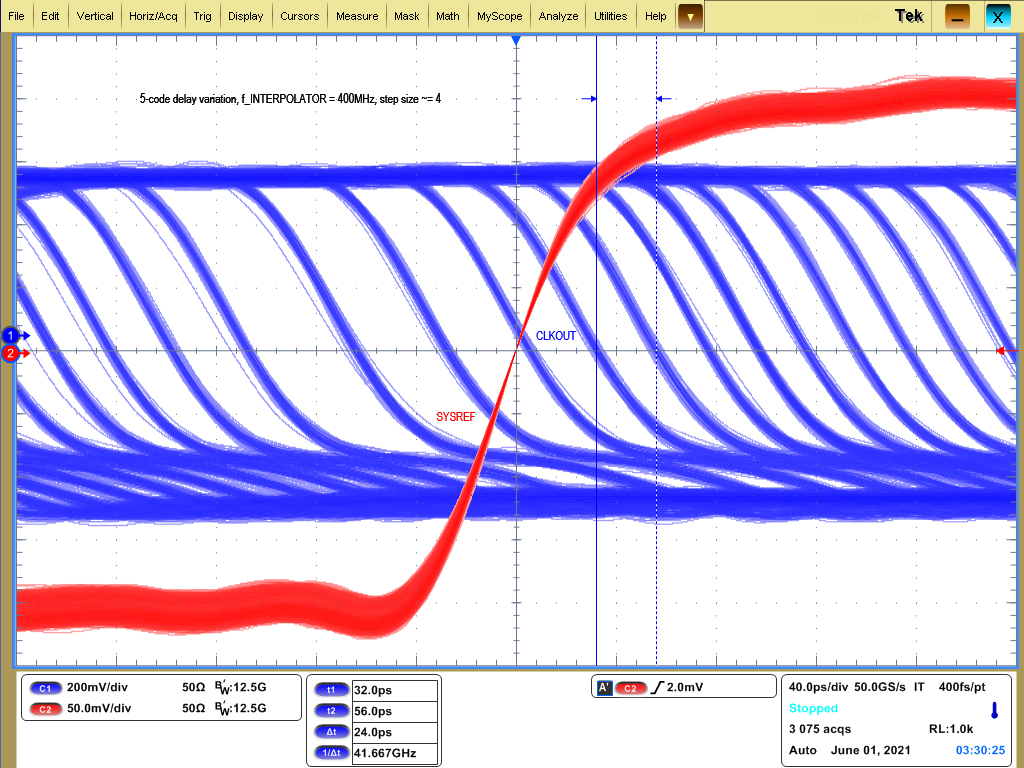
In generator modes, the SYSREF can be delayed by picosecond-size steps to more closely meet setup and hold requirements for high-frequency clock outputs. A delay divider, SYSREF_DLY_DIV, generates the interpolator frequency fINTERPOLATOR, which is usually in the range of 400 MHz to 800 MHz. This interpolator frequency is further subdivided into 512 delay codes, allowing approximately 2.5-ps to 5-ps delay steps across most of the CLKIN frequency range.
Each channel has its own delay codes which can be entered. The delay code algorithm is documented in the data sheet. To simplify delay calculation, the GUI provides an estimated relative delay: enter the relative delay, and the GUI will calculate the correct step values to achieve the requested delay as closely as possible. Alternately, the register-based delay fields can be stepped through or programmed to achieve the same result.
 Figure 3-7 SYSREF Delay, in 5-Code Steps