SNAU266A July 2021 – August 2022
4 Schematic
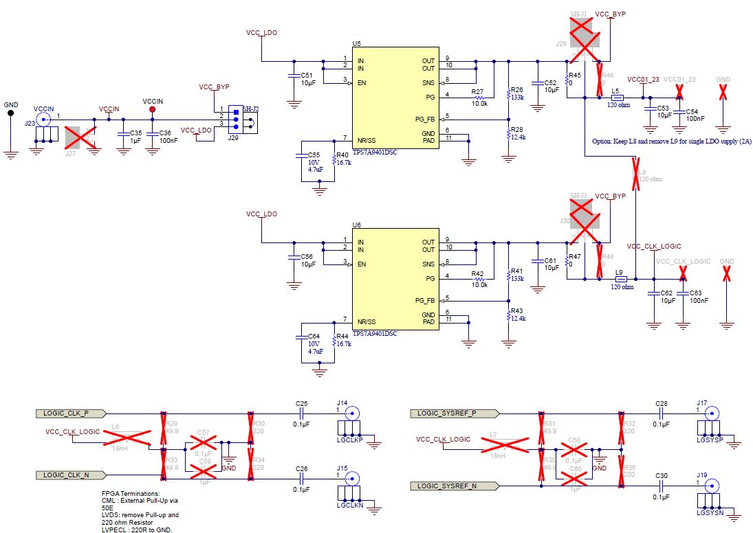 Figure 4-1 Schematic - Power
Supply
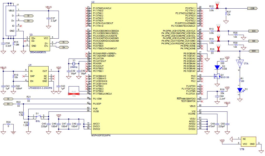 Figure 4-2 Schematic - LMX1204
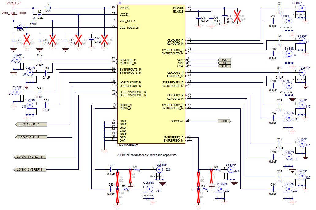 Figure 4-3 Schematic - USB2ANY
SNAU266A July 2021 – August 2022
 Figure 4-1 Schematic - Power
Supply
 Figure 4-2 Schematic - LMX1204
 Figure 4-3 Schematic - USB2ANY