SNAU266A July 2021 – August 2022
3.1 Buffer, Divider, and Multiplier Modes
From the top-menu, click Default Configuration → 800MHz Buffer Mode. This will automatically load the buffer mode profile.
 Figure 3-1 Loading the Default Configuration
If termination is not applied on all output pins, manually disable the unused outputs using the CHx_EN fields (to completely power down unused channels) or the CLKOUTx_EN, SYSOUTx_EN, and LOGICLK_EN/LOGISYS_EN fields (to power down output buffers only). Powering down unused channels greatly reduces current consumption, and for the logic clocks in particular can reduce spurious interference.
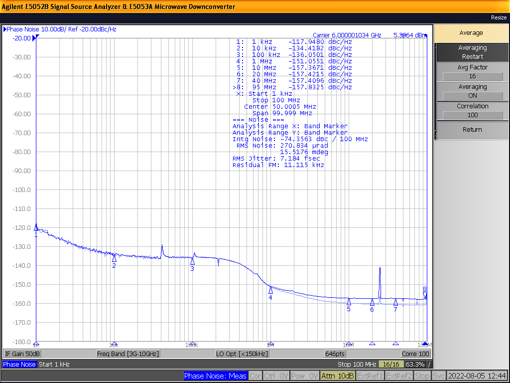
After the profile is loaded and any changes required have been made, the signal analyzer should see an 6000-MHz signal at around +6-dBm single-ended, or +9-dBm differential.
 Figure 3-2 6000-MHz Buffer Mode Signal Analyzer Plot
To activate the multiplier or the divider, change the CLK_MUX field to specify divider or multiplier modes, and change the CLK_DIV and CLK_MULT fields to specify the frequency scaling factor. To ensure the device cleanly enters each mode, first the desired configuration should be prepared in the GUI, then from the User Controls page the device should be reset by toggling the RESET field, and finally the registers should be reloaded using the USB Communications → Write All Registers menu option, or by pressing the accelerator keys CTRL + L.
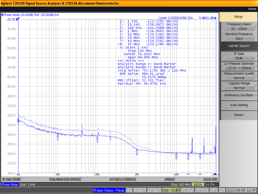
 Figure 3-3 3000-MHz Divide-by-2 Mode Signal Analyzer Plot
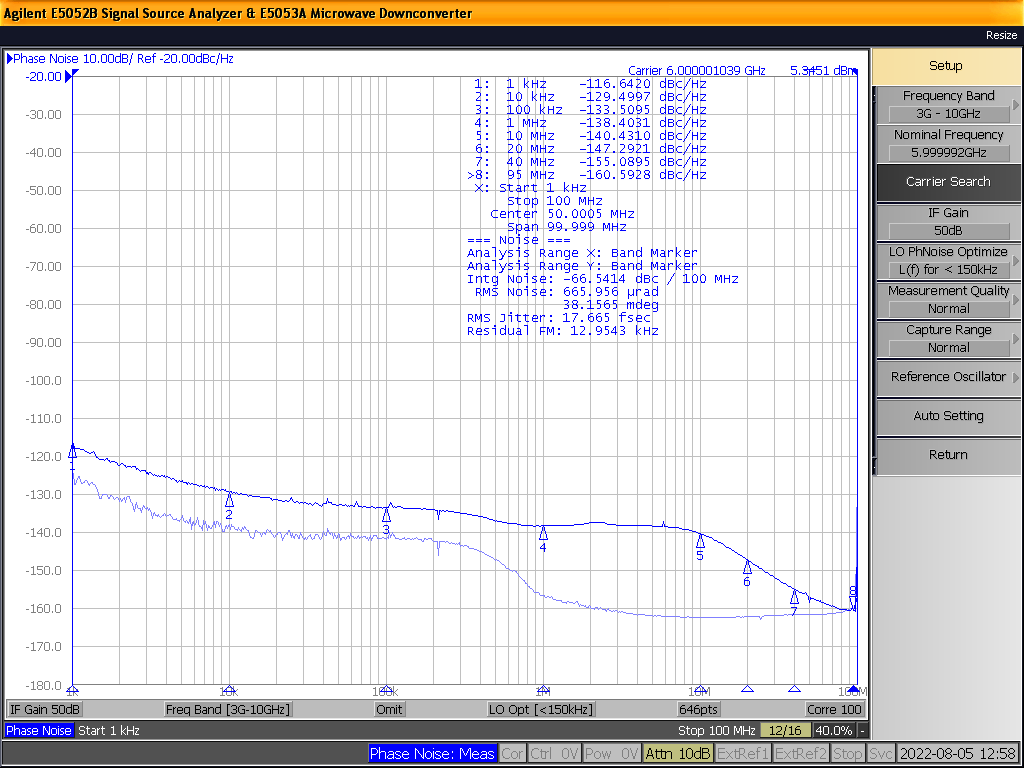
 Figure 3-4 6000-MHz Multiplier x2 Mode Signal Analyzer Plot