SNLA356 September 2020 DS90UB941AS-Q1 , DS90UH941AS-Q1
3 Bring-Up and Debug Flow
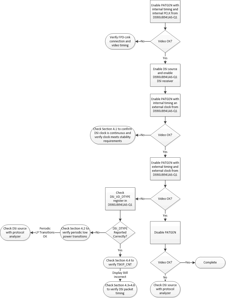
The following section describes a common debug flow that can be applied to bring-up for the interface between DS90UB941AS-Q1 and a DSI source. The focus of this debug is on the MIPI DSI interface and assumes that the FPD-Link channel between DS90UB941AS-Q1 and the partner deserializer has been properly established.
 Figure 3-1 Example DS90UB941AS-Q1 System
 In this example, the DS90UB941AS-Q1 is configured for DSI reference clock mode. For more information on configuring PATGEN from the DS90UB941AS-Q1, see Exploring the Int Test Pattern Generation Feature of FPDLink III IVI Devices.
 Figure 3-2 Recommended DS90UB941AS-Q1
Bring-Up Flow