SNLU317A september 2022 – may 2023 DP83867E
2.1 Components
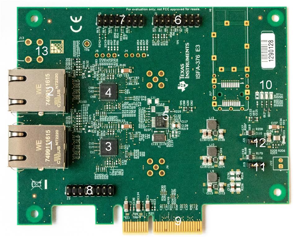
Figure 2-1 below gives a quick overview of the AIC board. The marked sections are described in the Table 2-1.
 Figure 2-1 Connectors, Jumpers and
LEDs
Figure 2-1 Connectors, Jumpers and
LEDsTable 2-1 Component Table
| Section | Description |
|---|---|
| 1 | RJ45 with integrated magnetic G-Bit network connection Port 1 / TSN_0 |
| 2 | RJ45 with integrated magnetic G-Bit network connection Port 2 / TSN_1 |
| 3 | DP83867 PHY1 for Port 1 |
| 4 | DP83867 PHY2 for Port 2 |
| 5 | 25 MHz clock generation for both PHYs |
| 6 | Signal connector MISC0 for validation |
| 7 | Signal connector MISC1 for validation |
| 8 | Signal connector RGMII interface (optional) |
| 9 | PCIe interface |
| 10 | Power indicator LEDs.
|
| 11 | VDDIO voltage selector jumper
pin-header
|
| 12 | VDDIO voltage selector jumper
pin-header
|
| 13 | Shield/Earth GND for testing. |