SNOAA68 June 2021 LMG3410R050 , LMG3410R070 , LMG3410R150 , LMG3411R050 , LMG3411R070 , LMG3411R150 , LMG3422R030 , LMG3422R050 , LMG3425R030 , LMG3425R050 , LMG3522R030-Q1 , LMG3526R030
5 Achieving Lifetime Switching
Power semiconductor devices need to be engineered to withstand hot-carrier effects occurring during switching. Tests used for Si FET reliability and robustness are not applicable to GaN FETs due to structural and material differences. For example the Hot Carrier Injection (HCI) test for lateral power FETs is not useful because the GaN FET has an electrically blocking buffer, and the Unclamped Inductive Switching (UIS) test could cause damage. JEP180 addresses this aspect, and in this section, we will show how TI GaN has been validated to be reliable for switching applications.
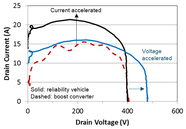
We apply accelerated hard-switching stress, per JEP180, using the continuous switching test-vehicle circuit of Figure 2-1 (per JEP182). Figure 5-1 shows how switching stress may be accelerated vs. that experienced under normal operation. The figure shows the switching locus curve or turn-on trajectory of a boost converter (dashed curve) operating at a bus voltage of 400 V and an inductor current of 5 A. The solid loci are from the test-vehicle circuit in Figure 2-1, at bus voltages and inductor currents of 400 V, 15 A and 480 V, 5 A showing current and voltage acceleration respectively.
 Figure 5-1 The
test-vehicle circuit in Figure 2-1 is used to apply
accelerated hard switching stress, illustrated by the
switching locus curves.
Figure 5-1 The
test-vehicle circuit in Figure 2-1 is used to apply
accelerated hard switching stress, illustrated by the
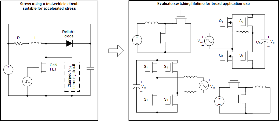
switching locus curves.We ran accelerated lifetime testing for voltage, current, temperature and frequency and generated a model as described in reference 19. Our approach calculates the switching stress by integrating the switching waveform while applying the voltage and current acceleration factors. This allows the complexity of the switching transition to be addressed. It enables stress to be applied using a suitable test-vehicle circuit, and for the switching lifetime to be calculated for broad application use as shown in Figure 5-2.
 Figure 5-2 Our switching
lifetime methodology allows for accelerated switching stress
to be applied by a test-vehicle circuit, and the switching
lifetime to be calculated for broad application
usage.
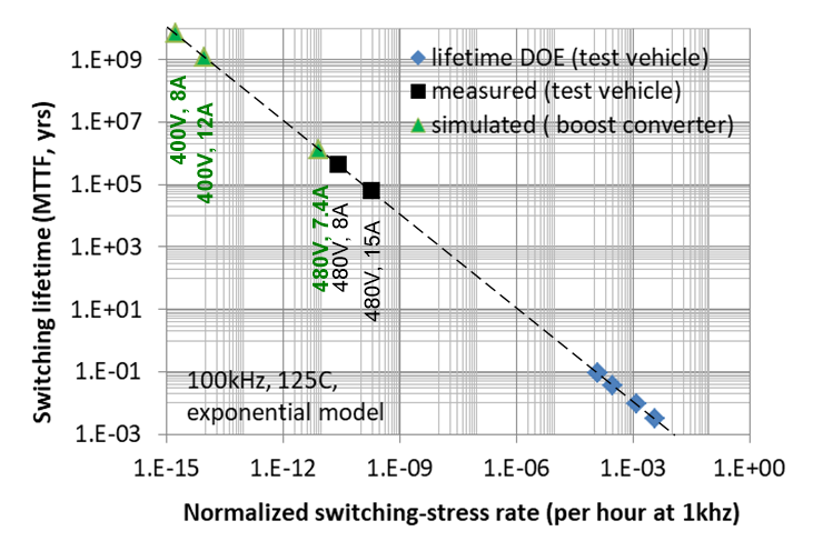
 Figure 5-3 Switching
lifetime MTTF calculation from both measured and simulated
waveforms (black and green points). The blue points
represent the lifetime run of DOE. The device is very
reliable for hard switching.
Figure 5-3 Switching
lifetime MTTF calculation from both measured and simulated
waveforms (black and green points). The blue points
represent the lifetime run of DOE. The device is very
reliable for hard switching.The model is used to calculate a normalized switching stress rate as shown in Figure 5-3, from which the lifetime for any given application operation can be determined. Both measured and simulated waveforms can be used, providing tremendous flexibility. The model can also be used in the calculation of time-varying stress, for example, for a PFC with AC line cycle as shown in reference 19. A Mean Time to Failure (MTTF) of 8.46 × 10⁹ yrs was calculated for a LMG3410R070 (70 mΩ) Integrated GaN FET Power Stage switching at 100 kHz (100 V/ns), with 400 V output, 8 A RMS inductor current in Continuous Conduction Mode (CCM). With 230 V RMS AC line input (1.84 kW). The high MTTF assures that there will be no intrinsic failure due to hot-electron wear out from hard-switching stress during regular operation.