SNVA991 October 2022 LM5123-Q1
- How to Design a Boost Converter Using LM5123
- Trademarks
- 1Design Example
-
2Calculations and Component Selection
- 2.1 Switching Frequency
- 2.2 Initial Inductor Calculation
- 2.3 Current Sense Resistor Selection
- 2.4 Inductor Selection
- 2.5 Output Capacitor Selection
- 2.6 Input Capacitor Selection
- 2.7 Feedback Resistor Selection
- 2.8 UVLO Resistor Selection
- 2.9 Soft-Start Capacitor Selection
- 2.10 Control Loop Compensation
- 2.11 MOSFET selection
- 3Implementation Results
- 4Small Signal Frequency Modeling
- 5Resources
2.7 Feedback Resistor Selection
The LM5123 controls the load voltage by the voltage on the TRK pin. The TRK pin is the reference voltage to the internal error amplifier. There are two output voltage ranges, a low range which allows for an output voltage range from 5-V and 20-V, and a high range which allows for an output voltage range from 20-V to 57-V. The range is selected by the resistance connected from the VREF pin to AGND. The VREF pin is a 1 V reference and is used to set a fixed load voltage through a resistor divider to the TRK pin. Table 2-1 shows the resistor range to select the voltage range. It is recommend to place a 470 pF capacitor from VREF to ANGD.
| Voltage Range | Minimum resistance | Maximum resistance | KFB(1) |
|---|---|---|---|
| Low range (5 V - 15V) | 75 kΩ | 100 kΩ | 20 |
| High range (20 V - 57 V) | 20 kΩ | 35 kΩ | 60 |
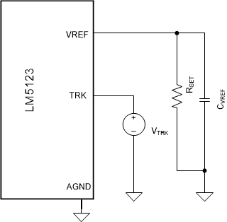
 Figure 2-3 Variable load voltage
configuration
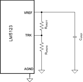
 Figure 2-4 Fixed load voltage
configuration
Figure 2-4 Fixed load voltage
configurationFor a variable load voltage the TRK pin voltage is set by an external source as shown in Figure 2-3.
The RSET resistance value is selected based on the require load voltage range. See Table 2-1 to select RSET. The TRK pin voltage for a given load voltage target is calculated using Equation 15.
To configure a fixed load voltage a resistor divider is connected from the VREF pin to the TRK pin as shown in Figure 2-4.
RVREFT is should be selected between the values calculated in Equation 16.
Assuming the target load voltage is 24 V, RVREFT must be between 12 kΩ and 21 kΩ. RVREFT is selected to be 21 kΩ. The value for RVREFB is calculated using Equation 17.
RVREFB is selected to be 14 kΩ.