SNVSB35B May   2018  – June 2020 LM26420-Q1

PRODUCTION DATA.  

  1. Features
  2. Applications
  3. Description
    1.     Device Images
      1.      LM26420 Dual Buck DC/DC Converter
      2.      LM26420 Efficiency (Up to 93%)
  4. Revision History
  5. Pin Configuration and Functions
    1.     Pin Functions: 16-Pin WQFN
    2.     Pin Functions 20-Pin HTSSOP
  6. Specifications
    1. 6.1 Absolute Maximum Ratings
    2. 6.2 ESD Ratings
    3. 6.3 Recommended Operating Conditions
    4. 6.4 Thermal Information
    5. 6.5 Electrical Characteristics Per Buck
    6. 6.6 Typical Characteristics
  7. Detailed Description
    1. 7.1 Overview
    2. 7.2 Functional Block Diagram
    3. 7.3 Feature Description
      1. 7.3.1 Soft Start
      2. 7.3.2 Power Good
      3. 7.3.3 Precision Enable
    4. 7.4 Device Functional Modes
      1. 7.4.1 Output Overvoltage Protection
      2. 7.4.2 Undervoltage Lockout
      3. 7.4.3 Current Limit
      4. 7.4.4 Thermal Shutdown
  8. Application and Implementation
    1. 8.1 Application Information
      1. 8.1.1 Programming Output Voltage
      2. 8.1.2 VINC Filtering Components
      3. 8.1.3 Using Precision Enable and Power Good
      4. 8.1.4 Overcurrent Protection
    2. 8.2 Typical Applications
      1. 8.2.1 2.2-MHz, 0.8-V Typical High-Efficiency Application Circuit
        1. 8.2.1.1 Design Requirements
        2. 8.2.1.2 Detailed Design Procedure
          1. 8.2.1.2.1 Custom Design With WEBENCH® Tools
          2. 8.2.1.2.2 Inductor Selection
          3. 8.2.1.2.3 Input Capacitor Selection
          4. 8.2.1.2.4 Output Capacitor
          5. 8.2.1.2.5 Calculating Efficiency and Junction Temperature
        3. 8.2.1.3 Application Curves
      2. 8.2.2 2.2-MHz, 1.8-V Typical High-Efficiency Application Circuit
        1. 8.2.2.1 Design Requirements
        2. 8.2.2.2 Detailed Design Procedure
        3. 8.2.2.3 Application Curves
      3. 8.2.3 LM26420-Q12.2-MHz, 2.5-V Typical High-Efficiency Application Circuit
        1. 8.2.3.1 Design Requirements
        2. 8.2.3.2 Detailed Design Procedure
        3. 8.2.3.3 Application Curves
  9. Power Supply Recommendations
  10. 10Layout
    1. 10.1 Layout Guidelines
    2. 10.2 Layout Example
    3. 10.3 Thermal Considerations
      1. 10.3.1 Method 1: Silicon Junction Temperature Determination
      2. 10.3.2 Thermal Shutdown Temperature Determination
  11. 11Device and Documentation Support
    1. 11.1 Device Support
      1. 11.1.1 Third-Party Products Disclaimer
      2. 11.1.2 Custom Design With WEBENCH® Tools
    2. 11.2 Documentation Support
      1. 11.2.1 Related Documentation
    3. 11.3 Receiving Notification of Documentation Updates
    4. 11.4 Support Resources
    5. 11.5 Trademarks
    6. 11.6 Electrostatic Discharge Caution
    7. 11.7 Glossary
  12. 12Mechanical, Packaging, and Orderable Information

Power Supply Recommendations

The LM26420-Q1 is designed to operate from an input voltage supply range between 3 V and 5.5 V. This input supply must be well regulated and able to withstand maximum input current and maintain a stable voltage. The resistance of the input supply rail must be low enough that an input current transient does not cause a high enough drop at the LM26420-Q1 supply voltage that can cause a false UVLO fault triggering and system reset. If the input supply is located more than a few inches from the LM26420-Q1, additional bulk capacitance can be required in addition to the ceramic bypass capacitors. The amount of bulk capacitance is not critical, but a 47-μF or 100-μF electrolytic capacitor is a typical choice.

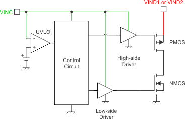
The LM26420-Q1 contains a high-side PMOS FET and a low-side NMOS FET as shown in Figure 42. The source nodes of the high-side PMOS FETs are connected to VIND1 and VIND2, respectively. VINC is the power source for the high-side and low-side gate drivers. Ideally, VINC is connected to VIND1 and VIND2 by an RC filter as detailed in VINC Filtering Components. If VINC is allowed to be lower than VIND1 or VIND2, the high-side PMOS FETs can be turned on regardless of the state of the respective gate drivers. Under this condition, shoot through will occur when the low-side NMOS FET is turned on and permanent damage can result. When applying input voltage to VINC, VIND1, and VIND2, VINC must not be less than VIND1,2 – VTH to avoid shoot through and FET damage.
LM26420-Q1 fig 42_snvsb35.gifFigure 42. VINC, VIND1, and VIND2 Connection